Diodes|Basic
What is a pn junction?
2026.05.13
A pn junction refers to a representative semiconductor structure formed by joining a p-type semiconductor and an n-type semiconductor. When an external voltage is applied across the junction, it exhibits rectifying behavior, allowing current to flow in only one direction, and this property is used to create many semiconductor devices, such as diodes and transistors. A familiar example is the LED: it applies the principle that electrons and holes recombine at the pn junction and emit light. This article explains the mechanism and characteristics of the pn junction in a way that beginners can understand.
Basic Understanding of p-type and n-type Semiconductors
In semiconductor materials such as silicon or germanium, adding impurity ions (doping) can significantly change their electrical properties. To understand a pn junction, it is important to grasp the characteristics of both the p side and the n side.
Characteristics of p-type Semiconductors
A p-type semiconductor contains holes (positive charge carriers) as the majority carriers. Specifically, when trivalent elements like boron are added to a tetravalent material such as silicon, there is a deficiency of electrons in the valence band, creating holes.
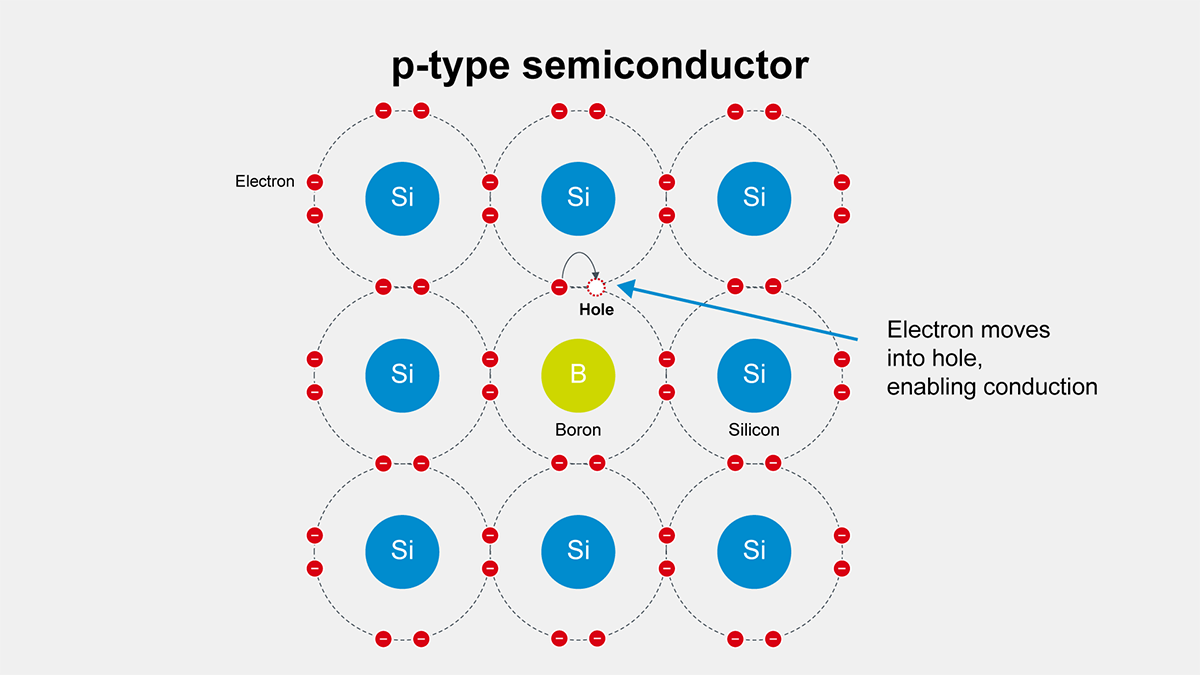
- By adding impurities, holes become the majority carriers
In p-type material, a trivalent impurity leads to “missing electrons,” and these vacancies act as holes with positive charge. - Representative p-type material and an outline of hole mobility
Silicon doped with boron conducts using holes, which generally have lower mobility than electrons. As a result, under the same doping level, p-type material typically has a slightly lower conductivity than n-type material.
Understanding these properties helps you visualize how holes move within the pn junction later.
Characteristics of n-type Semiconductors
In an n-type semiconductor, electrons serve as the majority carriers. Typically, pentavalent elements such as phosphorus or arsenic are added to silicon to increase the number of free electrons and enhance conductivity.
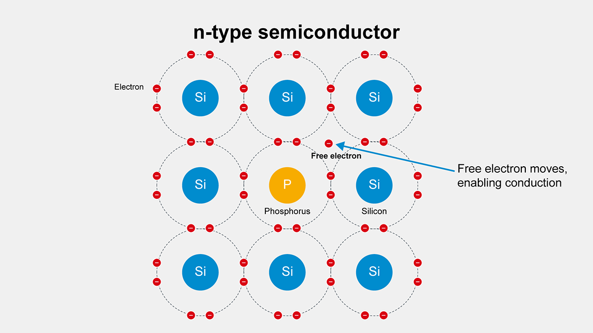
- By adding impurities, electrons become the majority carriers
A pentavalent impurity donates an extra electron that can move freely, making the n-type material rich in electrons. - Representative n-type material and an outline of electron mobility
When phosphorus is added to silicon, an extra electron remains after forming the crystal lattice bonds. Because electron mobility is often higher than hole mobility, the n-type region can exhibit greater conductivity than the p-type region at the same impurity concentration.
Increasing the impurity concentration increases the carrier concentration and, in turn, usually improves conductivity. However, if the concentration becomes too high, carrier mobility decreases, and further improvements in conductivity are limited. As a result, achieving an optimal balance of impurity concentration is crucial in practical manufacturing.
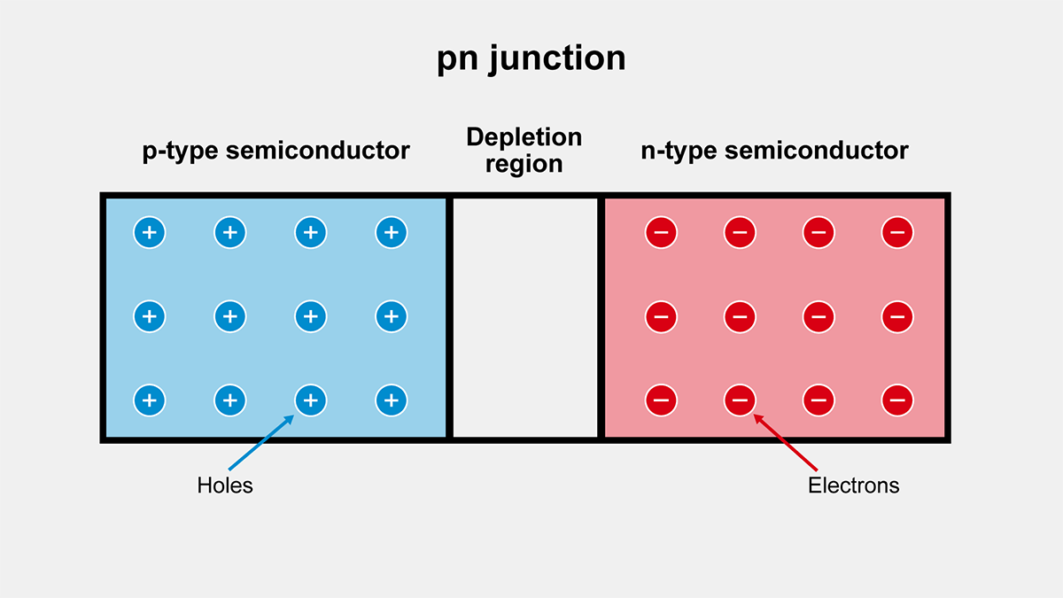
Formation of the pn junction and the Depletion Layer
A pn junction is a structure formed when p-type and n-type regions come into contact within a single semiconductor crystal. At this junction, electrons and holes diffuse and recombine, creating a carrier-depleted region, the depletion layer, and establishing a built-in potential. This characteristic serves as the fundamental principle underlying the operation of electronic devices such as diodes and transistors.
Mechanism of pn Junction Formation
When a p-type region and an n-type region are joined in a single crystal, numerous charge carriers move near the junction. Holes (positive charge) in the p side move toward the n side, and free electrons in the n side move toward the p side. In the immediate vicinity of the junction, they recombine actively.
- Joining p-type material and n-type material in a single crystal
In practical manufacturing, a wafer is selectively doped to create localized p-type or n-type regions within a single crystal. This produces a continuous boundary where the p side and n side are next to each other.
- Charge carrier diffusion and recombination near the junction
Initially, holes from the p side and electrons from the n side intermingle and recombine, leaving a region near the junction that is almost completely depleted of free carriers.
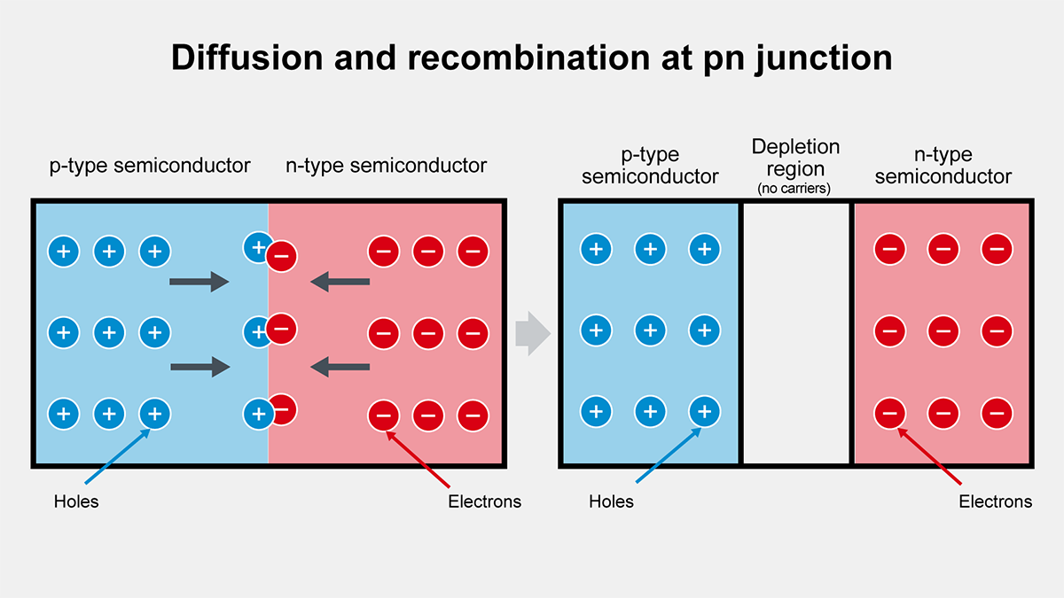
This process yields a depletion layer that defines the basic structure of the pn junction.
Depletion Layer and Built-in Potential
When the depletion layer forms, the ionized acceptor impurity remains on the p side, and the ionized donor impurity remains on the n side. This creates an electric field at the boundary.
- Formation of the depletion layer
The depletion layer contains almost no free carriers but retains fixed impurity ions. These charges produce an internal electric field that opposes further carrier diffusion. - The built-in potential (typically around 0.6–0.7V) that hinders carrier flow
In silicon, the built-in potential is typically 0.6-0.7V at room temperature. This prevents easy movement of carriers from one side to the other, so no large current flows without an external voltage.
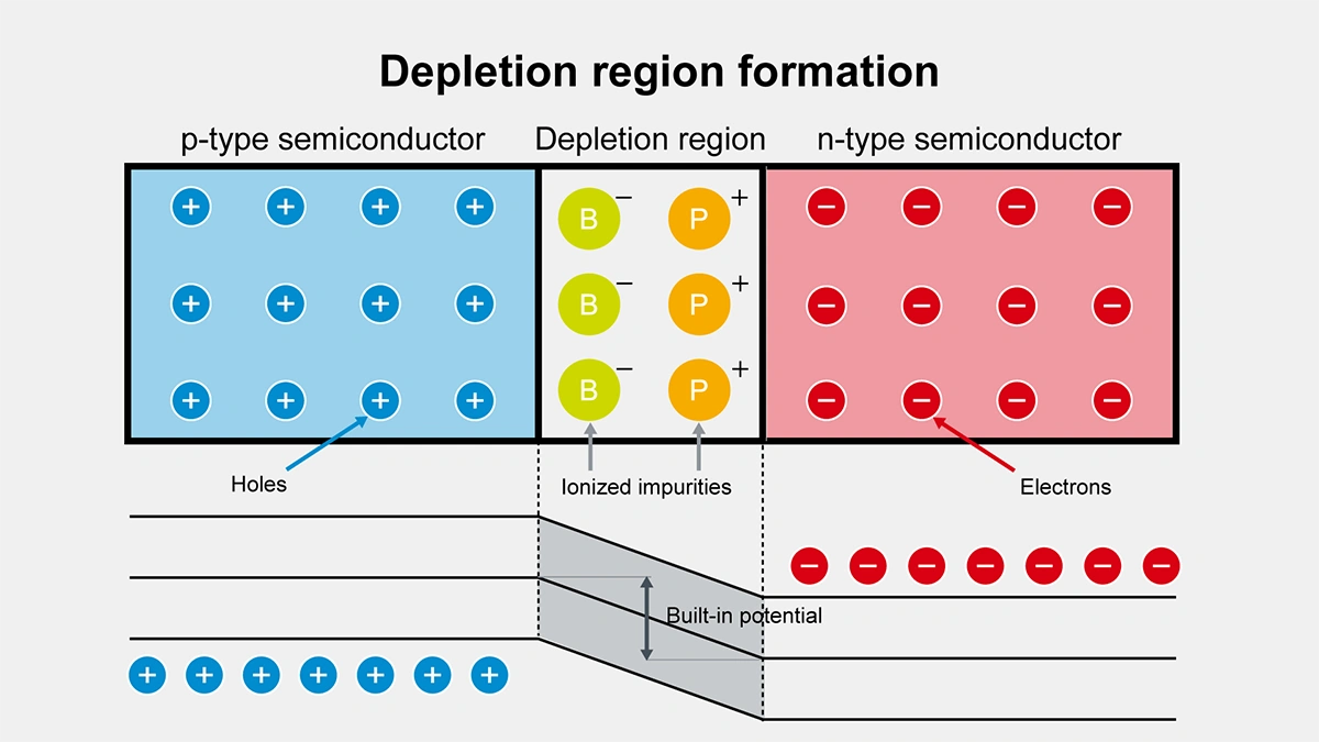
Because of this built-in potential that arises spontaneously, the pn junction demonstrates unidirectional conduction, providing the foundation for diode-type devices.
pn Junction Diode Operation
When an external voltage is applied across the pn junction, the thickness of the depletion zone and the net built-in potential change. As a result, current may or may not flow. Here we look at forward bias and reverse bias.
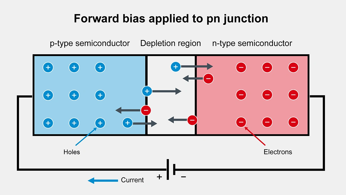
Forward Bias and Reverse Bias
Attaching the positive terminal to the p side and the negative terminal to the n side is called forward bias. The depletion layer narrows, allowing current to flow more easily in one direction.
- Under forward bias: The depletion layer narrows, and current flows easily
Applying a positive charge to the p side and a negative charge to the n side reduces the built-in potential difference, making it easier for majority carriers to cross the junction. If the forward voltage surpasses the built-in potential, a large current begins to flow.
- Under reverse bias: The depletion layer widens, resulting in minimal current (just leakage)
Applying the negative terminal to the p side and the positive terminal to the n side raises the built-in potential, blocking carrier flow. As a result, reverse current is limited to a very small leakage current, practically negligible in normal operation.
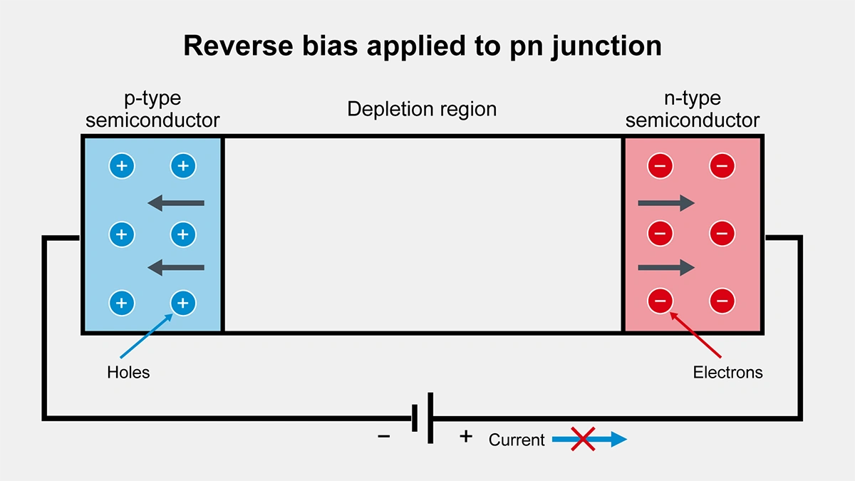
This property is key to functions like AC-to-DC conversion or switching in a pn junction diode.
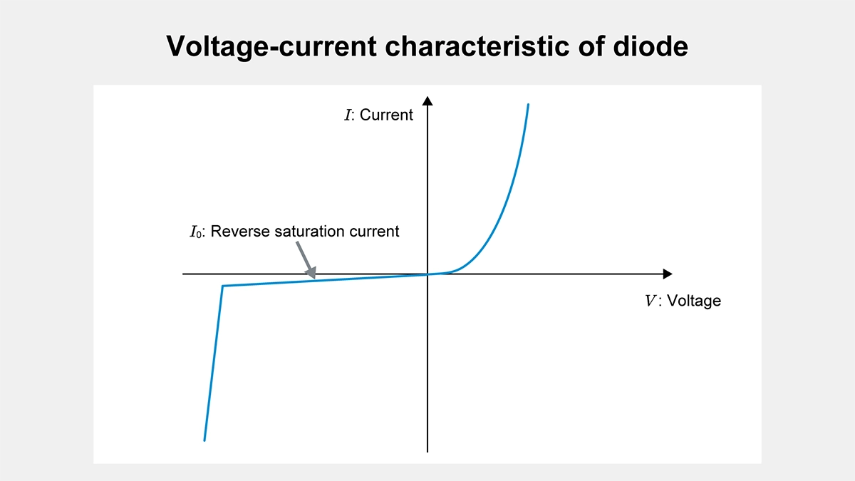
Current Characteristics and the Shockley Diode Equation
The current–voltage characteristic of a pn junction diode is often approximated by the Shockley diode equation:
\(I=I_0\begin{pmatrix} e^{qV/kT}-1\end{pmatrix}\)
where:
- I is the diode current
- I0 is the reverse saturation current
- q is the electronic charge (about 1.602 × 10⁻¹⁹ coulombs)
- V is the voltage across the diode
- k is the Boltzmann constant (about 1.38 × 10⁻²³ J/K)
- T is the absolute temperature (K)
- Overview of the Shockley Equation Derivation
We define the concentration of minority-carrier electrons within the p-type region as np(x), and the concentration of minority-carrier holes within the n-type region as pn(x). Under steady-state, one-dimensional, and low-level injection conditions, the following diffusion equation holds for minority electrons on the p-side:
\(D_n\displaystyle\frac{d^2Δn_p (x)}{dx^2}-\displaystyle\frac{Δn_p(x)}{τ_n}=0\)
Here, Δnp is the electron concentration in the p-type region, Dn is the electron diffusion coefficient, and τn is the average time before electrons recombine and disappear. A similar equation also applies to minority-carrier holes on the n-side.
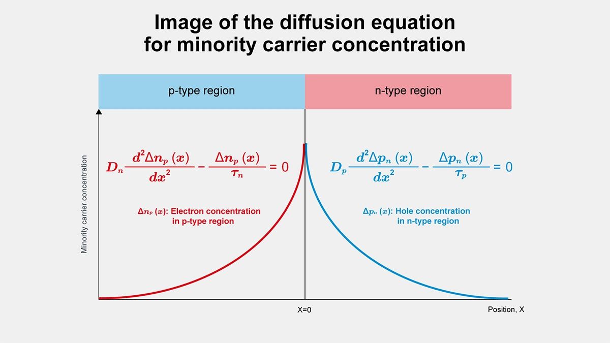
The solution to this second-order differential equation takes the exponential form:
\(Δn_p (x)=Δn_p (0)e^{-x/L_n}\)
Here, Ln is the electron diffusion length, defined by the following equation:
\(L_n=\sqrt{D_n τ_n}\)
The expression for Δpn(x) similarly becomes:
\(Δp_n (x)=Δp_n (0)e^{-x/L_p}\)
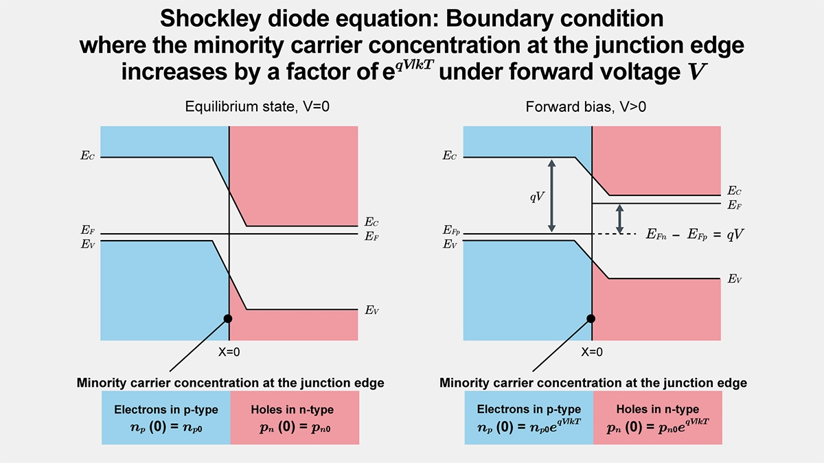
When a forward voltage V is applied, the junction barrier changes by an amount qV. According to Boltzmann statistics, the minority electron concentration at the junction edge on the p-side, np(0), is:
\(n_p (0)=n_{p0}e^{qV/kT}\)
Here, np(0) represents the equilibrium minority-carrier concentration.
Thus, the increment Δnp(0) is expressed as:
\(Δn_p (0)=n_p (0)-n_{p0}=n_{p0}\begin{pmatrix} e^{qV/kT}-1\end{pmatrix}\)
For minority-carrier holes in the n-type region, a similar relationship holds:
\(Δp_n (0)=p_{n0}\begin{pmatrix} e^{qV/kT}-1\end{pmatrix}\)
The electron diffusion current can be expressed as:
\(I_n=qAD_n\displaystyle\frac{dn_p (x)}{dx}|_{x=0}\)
Here, A is the cross-sectional area of the device through which current flows.
Since we are focusing on the magnitude rather than the direction of current, we treat currents as absolute values in subsequent calculations.
Since
\(np(x)=n_{p0}+Δn_p (x)\)
we obtain:
\(\displaystyle\frac{dn_p (x)}{dx}|_{x=0}=\displaystyle\frac{dΔn_p (x)}{dx}|_{x=0}=-\displaystyle\frac{Δn_p (0)}{L_n}\)
Therefore, using its magnitude, the electron current becomes:
\(I_n=qAD_n\displaystyle\frac{Δn_p (0)}{L_n}=qAD_n\displaystyle\frac{n_{p0}}{L_n}\begin{pmatrix} e^{qV/kT}-1\end{pmatrix}\)
Similarly, the hole diffusion current is expressed as:
\(I_p=qAD_p\displaystyle\frac{p_{n0}}{L_p}\begin{pmatrix} e^{qV/kT}-1\end{pmatrix}\)
The total diode current I is thus:
\(I=I_n+I_p=\begin{bmatrix}qA\begin{pmatrix}\displaystyle\frac{D_nn_{p0}}{L_n}+\displaystyle\frac{D_pp_{n0}}{L_p}\end{pmatrix}\end{bmatrix}\begin{pmatrix} e^{qV/kT}-1\end{pmatrix}\)
By defining the voltage-independent component as:
\(I_0=qA\begin{pmatrix}\displaystyle\frac{D_nn_{p0}}{L_n}+\displaystyle\frac{D_pp_{n0}}{L_p}\end{pmatrix}\)
We arrive at the Shockley diode equation:
\(I=I_0\begin{pmatrix}e^{qV/kT}-1\end{pmatrix}\)
Temperature Dependence
A pn junction diode’s behavior shifts with temperature. As lattice vibrations increase, collision probabilities also increase, affecting charge movement.
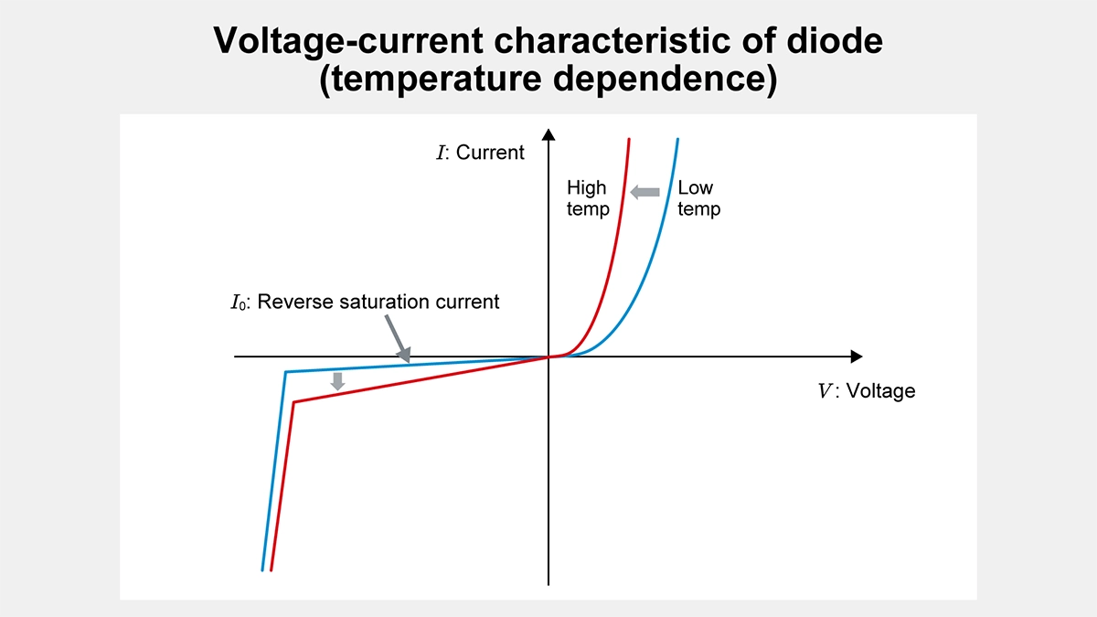
- Temperature characteristics of the built-in potential
In a silicon diode, the built-in potential tends to drop slightly as temperature rises. This is because greater thermal energy makes it easier for carriers to overcome the built-in potential. - Increased reverse current and changed operating characteristics
The reverse saturation current I0 increases with temperature, so at the same external voltage, the reverse current becomes larger. Designers must account for this leakage current and characteristic shifts in high-temperature environments.
Applications of the pn Junction Diode
Many devices are built on the behavior of the pn junction. Below are examples like Zener diodes and other types of diodes.
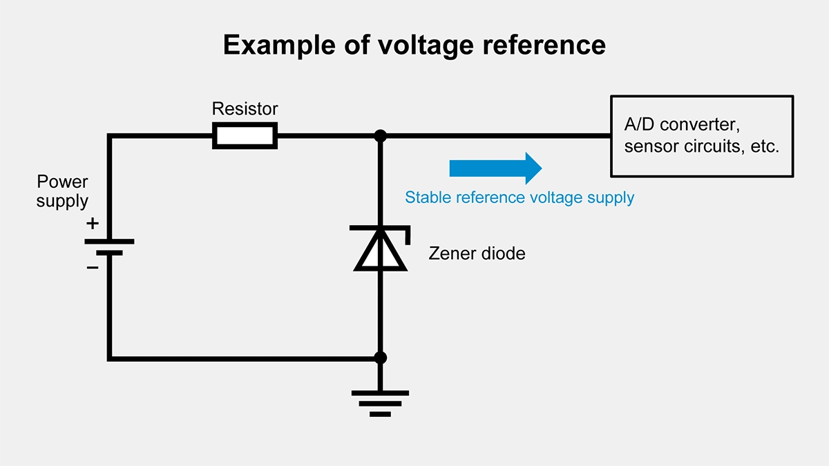
Voltage Regulation with a Zener Diode
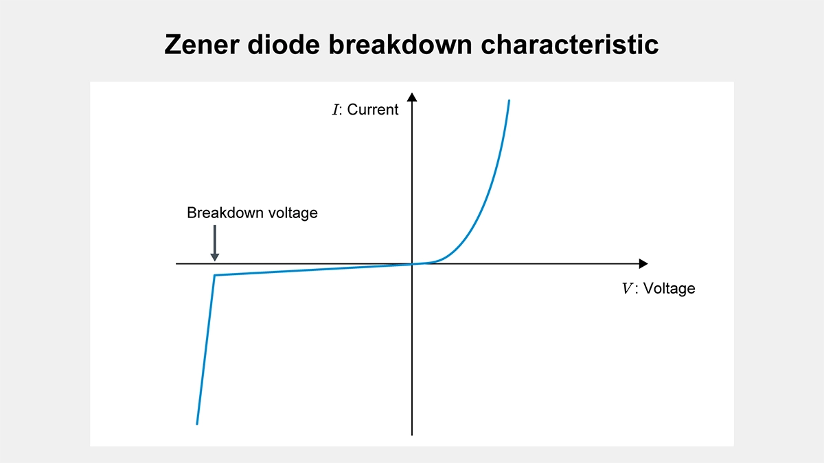
A Zener diode uses the breakdown voltage of the pn junction under reverse bias. Beyond a certain voltage, Zener breakdown happens abruptly, allowing a stable voltage reference.
- Zener breakdown under reverse bias
A heavily doped pn junction can be configured to break down at a relatively low voltage for steady operation.
- Power supply reference and overvoltage protection
Zener diodes provide a voltage reference and protect circuits from excessive voltage.
Both Zener and avalanche breakdown can occur. Depending on doping, one or the other dominates, but both are commonly referred to as Zener diodes.
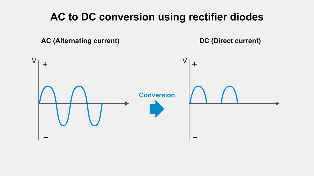
Other Uses of Diodes
One-directional conduction or reverse blocking at a pn junction is integral to a wide range of electronics.
- Rectifier diodes for AC–DC conversion
Alternating current can be converted to direct current by a diode bridge or a half-wave rectifier.
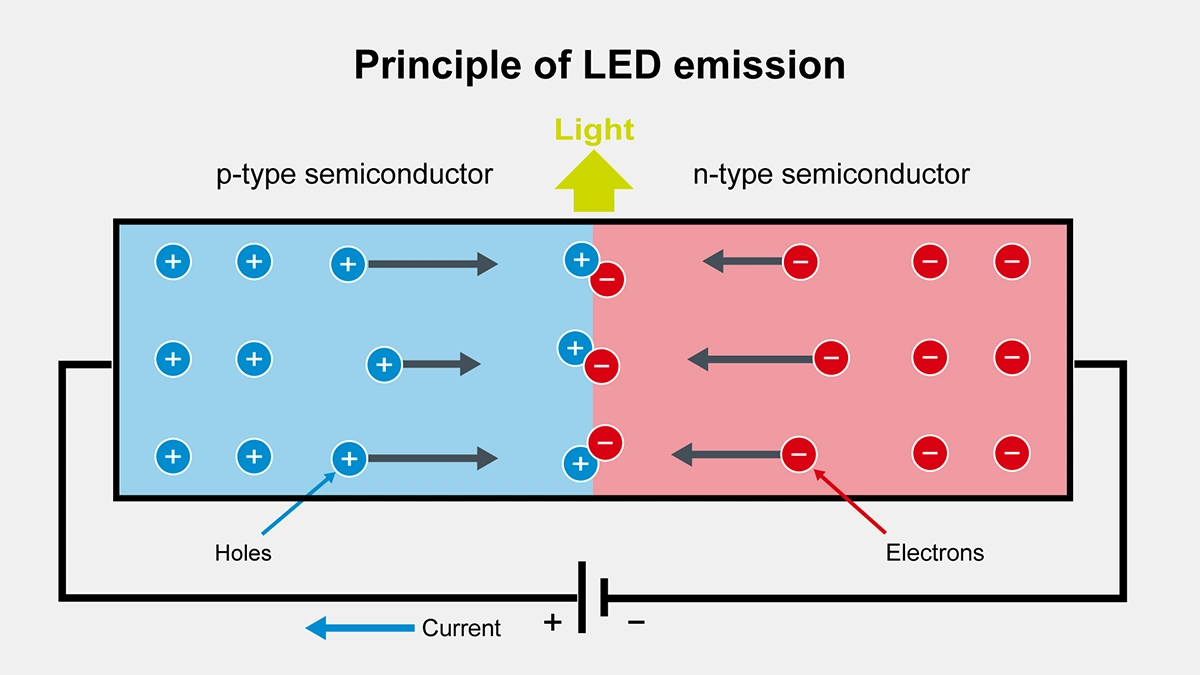
- Light-emitting diodes (LED) or laser diodes
Under forward bias, electrons and holes recombine, releasing light. Different semiconductor materials produce wavelengths from red to ultraviolet.
All such implementations rely on the inherent properties of the pn junction and play central roles across the electronics industry.
Summary
When a p-type material is joined to an n-type material in a single crystal, a depletion layer and a built-in potential form, giving the pn junction its unique electrical characteristics. Depending on the applied voltage (forward bias or reverse bias), the depletion zone width and built-in potential change, either allowing or blocking current flow.
This unidirectional conduction, often called diode action, underpins rectifiers, protection circuits, and light-emitting devices. Using the Shockley equation can quantify the current–voltage relationship and refine circuit designs.
Many devices, such as Zener diodes for voltage stabilization, are fundamentally based on the physics of the pn junction. A thorough understanding of how this junction works is essential for anyone involved in designing or analyzing electronic circuits.
Diodes
Basic
-
Diode Articles
- What is a pn junction?
- What Is a Diode? How It Works, Types, and Applications
- Rectifier Diodes
- Switching Diode
- Schottky Barrier Diodes (SBD)
- Zener Diode
- TVS Diodes
- PIN Diodes
- Diode Types and Characteristics: Static and Dynamic Characteristics, Current, Voltage, and Reverse Recovery Time
- Comparing Rectifier, Switching, Schottky, and Fast Recovery Diodes
- Schottky Diode Characteristics and Thermal Runaway
- Fast Recovery Diode (FRD) Characteristics
Evaluation