
Diodes|Basic
Schottky Diode (Schottky Barrier Diode)
2026.09.15
A Schottky diode—often referred to as a hot carrier diode—is built upon a metal semiconductor junction (the Schottky barrier) rather than the pn junction found in more traditional pn junction diodes. This distinctive construction enables fast switching speeds and a low forward voltage drop, making it highly attractive in power supply designs, digital circuits, and other high-frequency applications where low power dissipation and efficient waveform shaping are essential. You’ll often see Schottky diodes in DC-DC converters, switching regulators, and other circuits where reduced power dissipation and enhanced speed are critical. Understanding their unique properties—such as minority carriers playing a smaller role in conduction—helps with better component selection and more effective circuit design. Let’s dive deeper into the mechanism, structural features, and practical uses of the Schottky diode.
Fundamental Principles and Structure
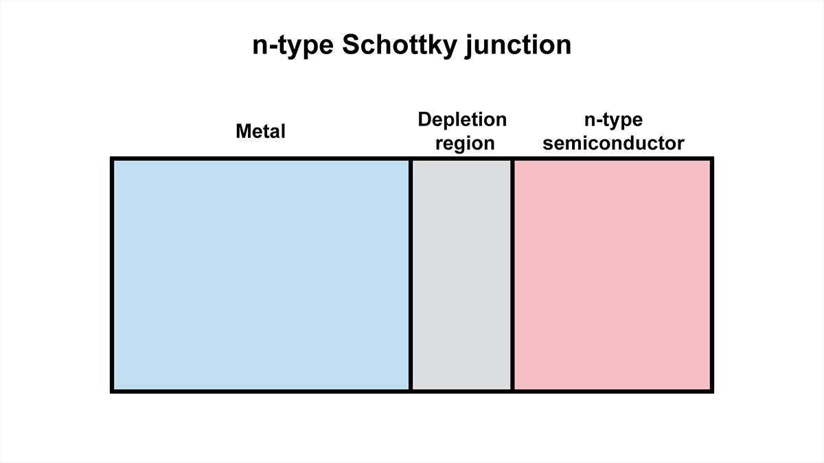
In a Schottky diode, a metal electrode (cathode or anode, depending on the package design) is in direct contact with an n-type semiconductor (or, in some rarer designs, p-type semiconductors). This results in a Schottky barrier that acts as the diode’s depletion region, setting it apart from a typical pn junction diode.
Metal-Semiconductor Junction and the Schottky Barrier
Unlike standard pn junction diodes, which rely on pn semiconductor junctions with majority and minority carriers diffusing across them, a Schottky diode forms at a metal-semiconductor junction. The difference between the metal work function and the semiconductor electron affinity produces a depletion region, also known as the Schottky barrier. This barrier determines how electrons move—or fail to move—in the forward direction or under reverse bias.
When a forward voltage is applied, electrons in the n-type semiconductor material can cross the barrier more directly, resulting in a smaller forward voltage drop compared to a typical pn junction diode. Because there is minimal minority carrier storage, Schottky diodes exhibit very fast switching and lower power loss during rapid changes in applied voltage. These unipolar devices are also sometimes called hot carrier diodes due to how electrons traverse the junction with relatively high energy.
\(Φ_{Bn}=Φ_{m}-χ\)
This simplified expression indicates how the barrier height ΦB depends on the metal’s work function Φm and the semiconductor’s electron affinity χ. By selecting different semiconductor materials (for instance, silicon carbide for high-voltage or high-temperature designs), one can alter this barrier and consequently optimize forward voltage drop, reverse leakage current, and other parameters.
Low Forward Voltage Drop
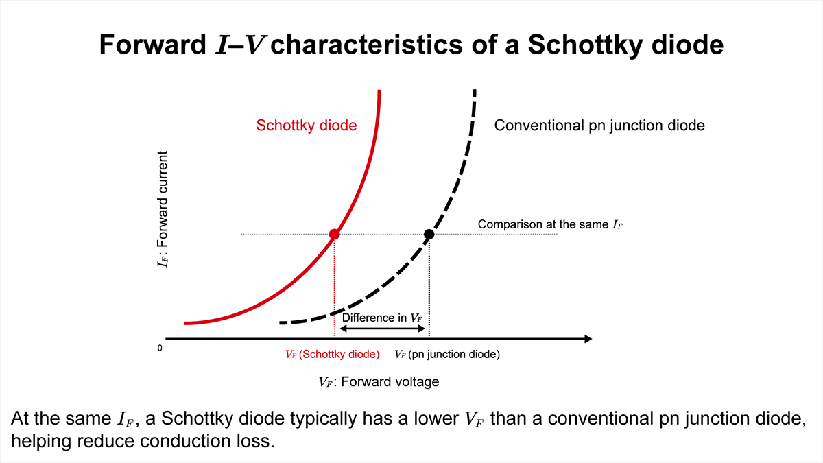
Schottky diodes typically have a lower forward voltage drop than conventional pn junction diodes. Compared to a traditional pn junction diode that might exhibit around 0.7 V, this low voltage drop helps limit power dissipation in the forward biased state. In lower-voltage power rails (e.g., 3.3 V or 5 V), every fraction of a volt saved can significantly reduce overall system losses.
Since there’s minimal junction capacitance associated with minority carriers, switching from forward to reverse conduction—or vice versa—happens quickly. This is particularly useful in high-frequency applications where fast switching is vital for efficiency, such as synchronous power supply designs, digital circuits, and wave-shaping tasks. That said, if large currents flow through the diode, it will still generate heat, so thermal considerations remain important in high power scenarios.
Fewer Minority Carriers and Fast Switching
In pn junction devices, minority carriers in the depletion region can accumulate, causing a longer reverse recovery time when switching from forward to reverse conduction. A Schottky diode largely avoids that pitfall because it’s dominated by majority carriers (electrons in an n-type material), leading to fast switching speed and lower overall power dissipation.
Still, these diodes are not universally perfect. Under higher reverse bias, the reverse leakage current can be greater than in a regular diode. Additionally, maximum reverse voltage (or breakdown voltage) may be lower, especially with basic silicon-based Schottky devices, though silicon carbide variants have pushed these limits significantly.
Electrical Characteristics and Key Parameters
When incorporating a Schottky diode into circuits, it’s essential to consider voltage ratings, reverse leakage current, power dissipation under load, and the required fast switching speed. Choosing the right device involves balancing the low forward voltage advantage against potential constraints on reverse bias capability and operating temperature.
Reverse Voltage Ratings
Many Schottky diodes are designed for moderate reverse voltages (e.g., up to 50 V). This is fine for many power supply outputs in the 5 V to 12 V range or various digital circuits that operate at low voltage. But if your design calls for higher voltages, you may need silicon carbide Schottky devices that withstand hundreds of volts while maintaining the hallmark small forward voltage drop.
Since metal semiconductor junctions have a shallower depletion region than their pn junction counterparts, electric field concentration can be higher, limiting maximum reverse voltage for standard Schottky types. By contrast, advanced silicon carbide diodes address that limitation, offering robust performance in high-power or high-voltage domains.
Reverse Leakage Current and Device Reliability
Direct metal contact that forms the Schottky barrier can allow increased reverse leakage current at higher temperatures. While negligible at room temperature, leakage may rise exponentially with ambient heat, potentially affecting digital circuits or precision analog stages if not accounted for. In power supply designs, especially where reliability is paramount, you want to ensure adequate thermal headroom.
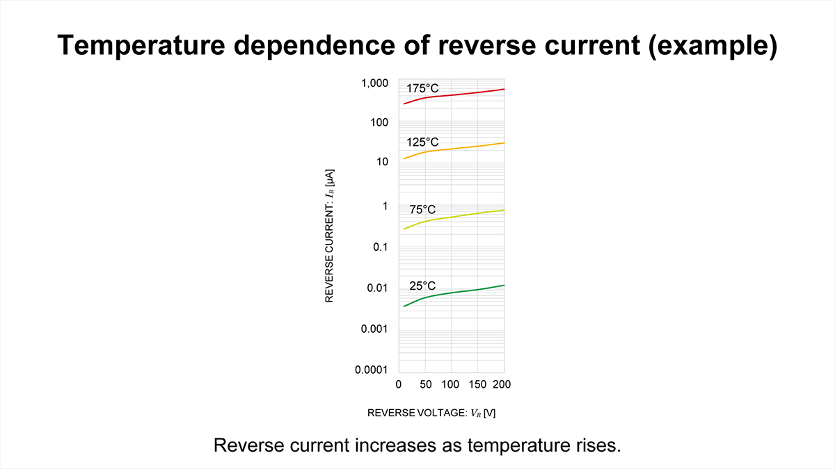
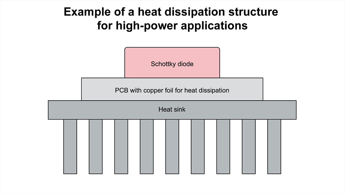
In harsh environments or high power applications, Schottky diodes might not be as rugged as some standard pn junction diodes regarding thermal runaway or surge conditions. So you’ll often see them used with heat sinks, higher copper area on the PCB, or specialized packages designed to handle larger amounts of power dissipation.
Fast Switching and Reverse Recovery Behavior
One reason Schottky diodes thrive in high-frequency power converters and waveform shaping circuits is their low stored charge, yielding fast switching with minimal reverse recovery time. Unlike a typical pn junction diode that may experience significant recovery delay when reversing polarity, the hot carrier diode can shift states extremely quickly, reducing losses in switching regulators or high-speed data lines.
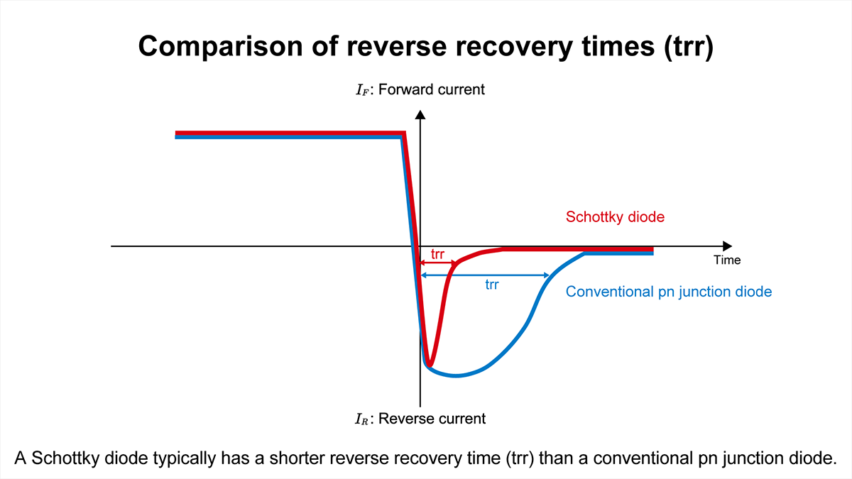
However, it’s still critical to address parasitic inductances on the board. Even if the diode itself can switch in the blink of an eye, stray inductances can cause voltage spikes or EMI issues. Techniques like snubber networks, careful routing of n-type or p-type connections, and mindful component layout help harness the diode’s inherent very fast switching behavior without incurring undue noise or overshoot.
Main Applications of Schottky Diodes
Thanks to their low voltage drop, fast switching speed, and stable unidirectional conduction, Schottky diodes appear in diverse circuits. Below are three prominent examples illustrating how you might leverage their unique properties.
Power Rectification and Loss Reduction in Power Supply Circuits
In power supply designs, Schottky diodes reduce conduction losses in the forward direction, making them ideal for the output stage of switching regulators. Because they have a low forward voltage drop, they help achieve better overall efficiency and produce less heat. This is particularly advantageous for low-voltage rails such as 3.3 V or 5 V, where every fraction of a volt can impact thermal design and battery life.
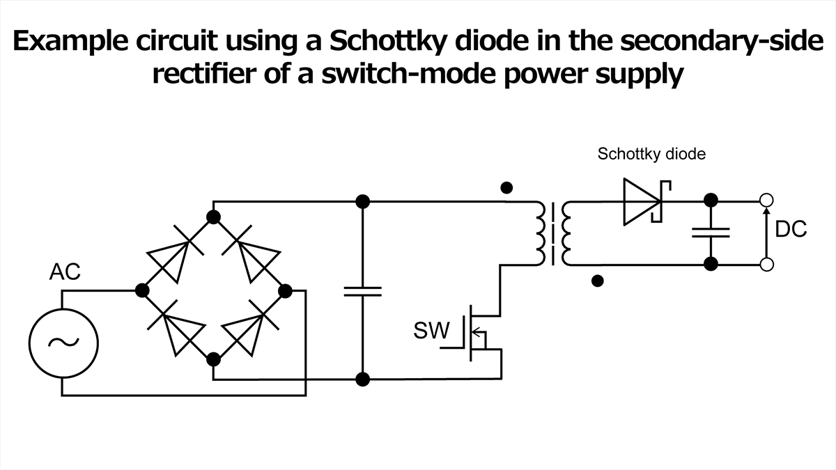
For high-frequency converters, Schottkys also provide extremely fast switching, minimizing reverse recovery losses. However, if the supply current is high, you’ll need to manage thermal aspects via adequate cooling. Proper junction temperature management ensures reliability and avoids runaway caused by power dissipation that can accumulate at elevated currents.
ESD Protection and Clamp Circuits
The Schottky diode symbol sometimes appears in circuits intended for ESD or transient protection because its low forward voltage can help quickly clamp or divert unwanted spikes. In transistor circuits, Schottky diodes may be used to prevent saturation—these are known as Schottky-clamped transistor configurations—helping to maintain faster switching in digital logic stages or waveform shaping paths.
Similarly, they work well as clamp diodes in circuits needing immediate conduction when voltages exceed certain thresholds. However, watch out for reverse leakage current if the clamp diode is subject to high temperatures or frequent transitions at high frequencies.
Reverse Current Blocking in Solar Panels
Schottky diodes are also highly regarded in solar power systems, particularly in photovoltaic modules. A diode is placed in series to prevent backflow from the battery or other panels when one panel has lower output (for instance, in partial shading). With a low voltage drop, a Schottky diode helps preserve the bulk of the generated power without significantly reducing efficiency.
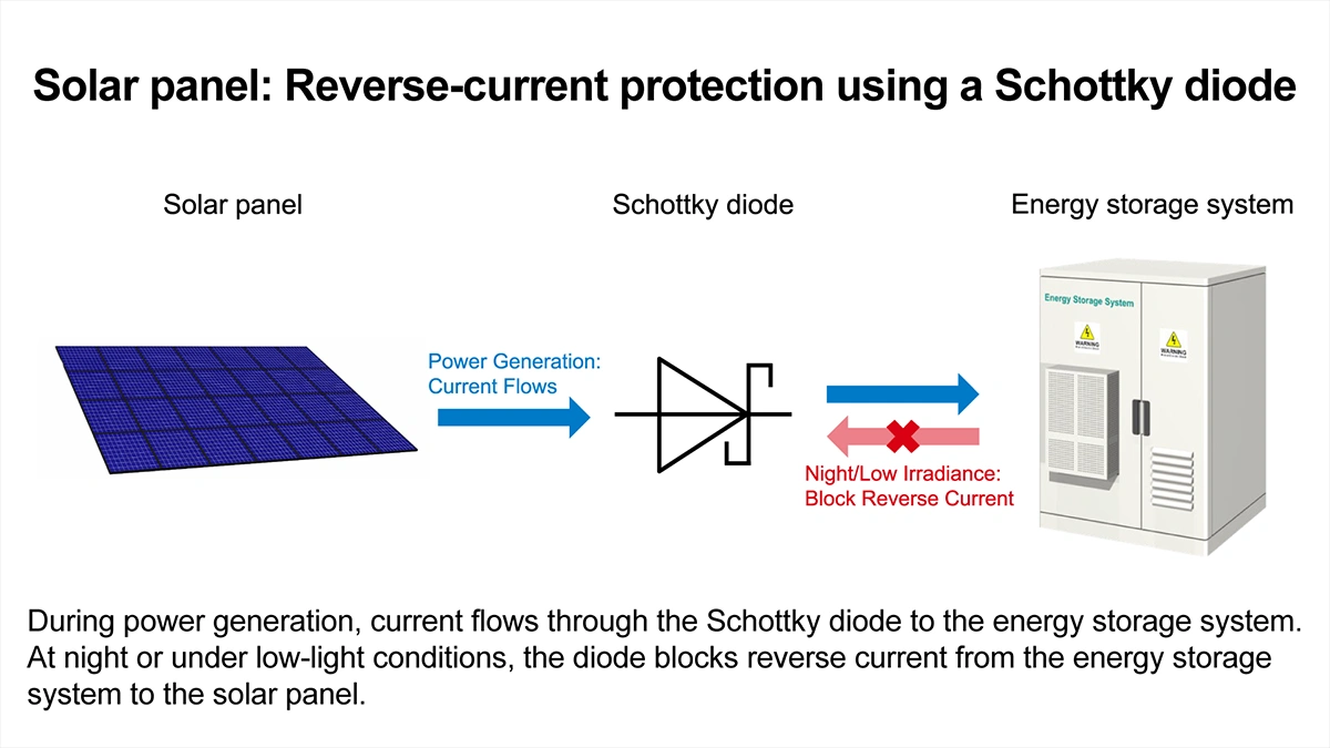
Outdoor conditions expose semiconductor junctions to wide temperature swings, so silicon carbide diodes with better thermal endurance sometimes become necessary for large-scale systems. The goal is to ensure that your n-type semiconductor material or the overall device package can handle the environment without excessive reverse leakage current or thermal degradation.
Points to Consider When Selecting and Using Schottky Diodes
While the Schottky barrier diode offers many advantages—less power wasted, fast switching, and a low voltage drop—designers should remember that higher reverse leakage, lower reverse voltage ratings, and thermal management are important trade-offs. Below are essential factors to keep in mind.
High-Power Usage and Thermal Management
When pushing a Schottky diode to handle high current or high voltage, examine specs such as maximum forward current and peak reverse voltage. A Schottky diode connected as a main rectifier in a high-wattage supply is likely to generate heat. Pairing it with an appropriate heat sink or a conduction-cooled design ensures the junction diode temperature remains within safe limits.
If you need a pn junction device for extreme voltages (hundreds of volts or more), you might opt for a silicon carbide Schottky diode. Standard Schottky diodes often max out at around 50 V, but SiC versions can go much higher while maintaining a relatively low forward voltage drop.
\(P_{F}\approx V_{F} \times I_{F}\)
In this equation, PF is the forward conduction loss, VF is the forward voltage drop under the operating conditions, and IF is the forward current.
Remember that conduction losses, combined with the diode’s ohmic contacts, produce heat that can degrade device reliability if not managed.
Avoiding Static Damage and EMI Issues
Some designers use Schottky diodes as ESD or transient protectors. Yet, if the reverse bias from a static discharge exceeds the device rating, the diode can be damaged. Proper factory handling, ESD mats, wrist straps, and board-level protection measures remain important. You may also combine Schottky diodes with TVS diodes or clamp circuits to handle stronger surges safely.
At high frequencies, route your Schottky diode to minimize stray inductance. Even a diode with a fast switching speed can’t overcome board-level parasitic inductances that cause ringing or voltage spikes. Keeping lead lengths short, using ground planes effectively, and controlling loop areas will help ensure stable performance.
Summary
A Schottky diode (sometimes called a Schottky barrier diode or hot carrier diode) capitalizes on a metal-semiconductor junction instead of a pn junction, resulting in a low forward voltage drop and very fast switching characteristics. This makes it a prime choice for low voltage power rails, high-frequency switching applications, digital circuits, and any scenario where low power dissipation is crucial.
That said, designers should account for its lower reverse voltage thresholds and potentially higher reverse leakage current at elevated temperatures. Silicon carbide variants extend the range by enabling higher blocking voltages and improved thermal performance. By addressing thermal constraints, protective clamping, and matching the right Schottky diode to your applied voltage and current needs, you can enjoy substantial gains in efficiency and speed.
Careful circuit planning—factoring in reverse bias peaks, junction temperature, and potential surge events—will help you harness the unique properties of the Schottky diode without sacrificing reliability. Used correctly, Schottky diodes can significantly reduce power dissipation, simplify switching topologies, and improve performance in countless electronic designs.
【Download Documents】 Transistors & Diodes Basics and Selection
In this handbook, although there are so many types of power devices using Si semiconductors, the basic points are explained, focusing mainly on diodes and transistors for power supply applications. It also introduces the procedure and decision method for transistor selection when designing circuits, as well as application examples that utilize each characteristic and feature.
Diodes
Basic
-
Diode Articles
- What is a pn junction?
- What Is a Diode? How It Works, Types, and Applications
- Rectifier Diodes
- Switching Diode
- Schottky Diode (Schottky Barrier Diode)
- Zener Diode
- TVS Diodes
- PIN Diodes
- Diode Types and Characteristics: Static and Dynamic Characteristics, Current, Voltage, and Reverse Recovery Time
- Comparing Rectifier, Switching, Schottky, and Fast Recovery Diodes
- Schottky Diode Characteristics and Thermal Runaway
- Fast Recovery Diode (FRD) Characteristics
Evaluation