
Opamps|Basic
What Is an Operational Amplifier? Principles, Functions, and Differences from Comparators
An op amp, or operational amplifier, is an analog IC that amplifies and outputs the small voltage difference between two input pins. Because it has high input resistance and low output resistance, it can drive the next circuit stage without placing an unnecessary load on the signal source. By applying negative feedback, which returns part of the output to the input, the gain and operation can also be stabilized. Op amps are used in a wide range of circuits, including circuits that amplify the weak output of sensors and buffers, or voltage followers, that pass a signal to the next stage without degrading it. This article explains op amp operation, configuration and principles, roles in circuits, selection points, characteristics and terms, and the differences between op amps and comparators.
How Op Amps Work
First, we will look at how an op amp handles the voltage difference between its input pins and how negative feedback determines circuit operation. Before going into pin details and internal circuitry, we will cover the basic ideas through differential-voltage amplification, virtual short behavior, and voltage follower operation.
Amplifying the Voltage Difference Between Two Input Pins
This section looks at what an op amp treats as its input. The important point is not the voltage at the + input pin or the – input pin by itself, but the differential voltage that appears between the two input pins.
An op amp amplifies the small differential voltage between the + input pin and the – input pin and outputs the result. For this reason, an op amp is expected to have high gain.
If the same voltage is applied to both the + input pin and the – input pin, ideally there is no change in the output. The output is determined by the difference between the two inputs, and the output direction changes depending on which input is higher.
However, the open-loop gain of an op amp by itself is very large, so when it is used without negative feedback, the output can easily swing close to the supply voltage. In practical amplifier circuits, negative feedback is therefore configured with external resistors or other components so that the circuit provides the required gain.
Negative Feedback and Virtual Short
Because an op amp has very large open-loop gain, even a small voltage difference between its input pins can produce a large output change. If used as-is, the output can easily swing close to the supply voltage. Practical amplifier circuits therefore use negative feedback, returning part of the output to the – input pin, to set the required gain and operation.
Within the range where negative feedback is working correctly and the op amp is operating linearly, the output changes in the direction that reduces the potential difference between the + input pin and the – input pin. As a result, even though the two input pins are not physically connected, they can be treated as being at almost the same potential. This approximation is called a virtual short.
A virtual short is an idea that can be used when negative feedback is applied, sufficient loop gain is available, and the circuit remains within the input common-mode voltage range and output swing range. Negative feedback does not always guarantee stability. Oscillation or disturbed response can occur depending on bandwidth, phase margin, capacitive load, wiring, and board parasitics. The next section uses a voltage follower as a specific circuit example of this idea.
Basic Operation Seen in a Voltage Follower
The relationship between negative feedback and virtual short behavior is easier to understand by looking at a voltage follower. Here, we use a circuit that passes the input voltage directly to the output as an example and confirm why the output error becomes small when the open-loop gain is sufficiently large.
A voltage follower circuit is a negative feedback circuit in which the output pin is connected directly back to the – input pin. Within the range where the required conditions are satisfied, the output changes so that it follows the input voltage applied to the + input pin, and the input voltage and output voltage become nearly equal. The voltage gain is approximately 1x, but because the circuit takes advantage of high input resistance and low output resistance, it can pass the signal to the next stage as a voltage buffer.
Voltage follower circuit

In this circuit, because the output voltage is returned to the – input pin, the differential voltage between the input pins can be considered as VS–VOUT. The op amp amplifies this differential voltage by the open-loop gain AV, so the output voltage is expressed as follows.
\(V_{OUT} = A_V × (V_{IN+} – V_{IN-}) = A_V × (V_S – V_{OUT})\)
Therefore,
\(V_S – V_{OUT} = \displaystyle\frac{V_S}{1+A_V}\)
When the open-loop gain AV is sufficiently large, the differential voltage VS–VOUT, which corresponds to the left side of the equation, can be treated as a value close to 0, so VS=VOUT can be approximated. This does not mean that the input and output are exactly equal. Error can remain because of finite open-loop gain, input and output ranges, and load conditions.
High open-loop gain is desirable in an op amp because it helps make this error as small as possible. Seen another way, when negative feedback works correctly, the potential difference between the + input pin and the – input pin becomes small, making it easier to treat the inputs as the virtual short described in the previous section.
In a voltage follower, this property allows the circuit to keep the voltage gain at approximately 1x while reducing the load on the signal source and passing the signal to the next stage. However, the datasheet should be checked to confirm that the op amp used is unity-gain stable and does not oscillate with a capacitive load.
Op Amp Configuration and Principles
This section reviews the pin configuration seen from outside the op amp, the ideal model, and the role of the internal circuit. It organizes how the operation described in the previous chapter is produced by the pins, input stage, gain stage, and output stage.
Op Amp Pin Configuration and Supply Pin Names
When using an op amp, one of the first points that can cause confusion is which pins receive the signal and which pins connect to the power supply. Here, as a basis for reading circuit diagrams and datasheets, we confirm the basic pins and supply pin names for one circuit.
An op amp consists of five pins per circuit: a positive supply pin, a negative supply pin, a + input pin, a – input pin, and an output pin.
Note: In general, pin names are not standardized beyond the categories of power supply, input, and output.

| Bipolar type | CMOS type | |
|---|---|---|
| Positive supply pin | VCC | VDD |
| Negative supply pin | VEE | VSS |
Input Resistance and Output Resistance of an Ideal Op Amp
Next, we use the ideal model to confirm what kind of op amp does not place extra influence on the signal source or load. High input resistance and low output resistance are basic conditions for receiving a sensor signal without disturbing it and passing it to the next stage.
High input resistance (impedance) and low output resistance are required functions of an op amp. In the figure below, the voltage-controlled voltage source amplifier model, the relationship between the input voltage and output voltage is expressed by the following equation. Voltage-controlled voltage source amplifier model.


\(V_O = A_V × \displaystyle\frac{R_i}{R_i + R_S} × \displaystyle\frac{R_L}{R_O + R_L} × V_S\)
The signal voltage VS is divided by the signal source resistance RS and the op amp input resistance Ri, so an attenuated signal is input to the op amp. However, when Ri is sufficiently larger than RS (Ri=∞), the first term of the equation can be approximated as 1, and VS=Vi can be assumed. Next, for the second term, the amplified input voltage AVVi is divided by the op amp output resistance RO and the load resistance RL, and then output. At this time, if RO is sufficiently smaller than RL (RO=0), the second term can be approximated as 1, and the signal can be output without attenuation. This type of op amp is called an ideal op amp. Ordinary op amps are designed with circuit configurations that approach the ideal op amp, for which high input resistance and low output resistance are desirable.
| Input Resistance | Output Resistance | |
|---|---|---|
| Ideal Opamp (Voltage-Controlled Voltage-Source) |
∞ | 0 |
Internal Circuit Configuration
After confirming the pins and ideal model, we next look at which stages inside the IC the signal passes through as it is amplified. This is not for designing the internal circuit in detail, but for understanding how the input stage, gain stage, and output stage relate to op amp characteristics.
The internal circuit configuration of an op amp is shown below. In general, an op amp can be considered as having three stages: an input stage, a gain stage, and an output stage.
The input stage is configured as a differential amplifier stage and receives the differential voltage between the + input pin and the – input pin. A common-mode signal component, where the same voltage is input with no potential difference between the pins, is ideally suppressed, but in an actual IC this is a finite characteristic expressed as the common-mode rejection ratio.
The gain stage supplements the gain that is not sufficient from the differential amplifier stage alone and increases the overall open-loop gain of the op amp. In a typical op amp, phase compensation capacitance for preventing oscillation is connected around the gain stage so that the device can be used stably in negative feedback circuits.
The output stage reduces the influence of the load connected to the output pin and drives the next stage. Load-related distortion, voltage drop, and similar effects mainly depend on the output-stage circuit configuration and current capability. Output stages are classified as Class A, Class B, Class C, Class AB, and other types. Here, as an overview of the internal circuit, the key point is that the output stage is the part involved in driving the load.


Roles of an Op Amp
An op amp is used to convert a small voltage difference into a signal that is easier to handle and to separate the influence of the signal source and load so the circuit can operate stably.
In sensor and detection circuits, the signal source output is often small. If it is passed directly to a later A/D converter or control circuit, it can be affected by errors and load conditions. Using an op amp reduces the load on the signal source while adjusting the signal to the required voltage range and making it easier to pass to the next circuit.
Converting Small Signals into Easier-to-Use Voltages
Small signals obtained from sensors and detection circuits may be difficult for later circuits to handle as-is. An op amp plays the role of amplifying these small signals to the required voltage level.
For example, when the output of a sensor is read by an A/D converter or an A/D input built into a microcontroller, a signal that is too small relative to the input range cannot use the available resolution effectively. Amplifying the signal to an appropriate range with an op amp makes it easier for the next circuit to read signal changes. However, in addition to the required gain, offset, noise, input range, and output range must also be checked.
When amplifying a small signal, simply making it larger is not enough. Noise superimposed on the signal and input offset voltage are handled at the same time, so the gain and error factors must be considered together according to the resolution and measurement range required in the next stage.
Separating the Signal Source from the Load
The characteristics of high input resistance and low output resistance allow the load to be driven while reducing the burden on the signal source.
High input resistance makes it difficult to disturb the voltage of the signal source, while low output resistance makes it easier to drive the next circuit or load.
Some signal sources, such as sensors and voltage divider circuits, have high output resistance. If a load is connected directly to such a signal source, the signal source resistance and load resistance form a voltage divider, and the voltage you want to obtain may decrease.
When an op amp is inserted between the stages, almost no current is drawn from the previous stage, while the required current can be supplied more easily to the later stage. This function is especially important in buffer applications. In a voltage follower, even though the voltage gain is approximately 1x, the signal voltage can be passed to the next circuit while being maintained.
Applications in Measurement, Control, Audio, and Power Supplies
In measurement, control, audio, and power supply circuits, op amps are used for purposes such as signal amplification, buffering, and filtering. Depending on the application, input range, output range, noise, temperature characteristics, and other items must be checked.
In measurement circuits, sensor signals are adjusted to voltages that are easier to read. In control circuits, detected signals are shaped into forms that are easier to use for judgment and control. In audio circuits, op amps are used for signal amplification and filtering, and in power supply circuits they are used as signal-processing sections that support voltage and current detection and feedback control. Because the required accuracy, bandwidth, noise performance, and input/output ranges differ by application, the characteristics must be checked according to the circuit purpose.
How to Select an Op Amp
When selecting a type, check not only the power supply configuration but also whether the input signal falls within a usable range and whether the output can swing to the voltage required by the next circuit. Checking accuracy, noise, bandwidth, current consumption, operating temperature range, and related items according to the application also makes it easier to choose an op amp that fits the circuit conditions.
Selecting by Power Supply Configuration
The first point to check is whether the circuit can provide both positive and negative supplies or needs to operate from a single supply. The power supply configuration is related to the reference potential of the input signal and whether signals near 0V can be handled. However, the actual usable range is determined not only by the supply method but also by the input common-mode voltage range and output swing range, so the differences between dual supply and single supply should be understood and then confirmed in the datasheet.
Characteristics of Dual Supply Op Amps
Because op amps often amplify small signals close to 0V, when 0V input is required with a dual supply op amp, VEE is set on the negative voltage side. The required negative supply voltage differs depending on the product and the input common-mode voltage range, so it should be checked in the datasheet. Since a negative supply is used in many cases and both positive and negative supplies are required, these devices are called dual supply op amps.
Characteristics of Single Supply Op Amps
A single supply op amp is a type that can operate easily from a single supply without preparing a negative supply. Products that can handle signals near 0V are also called ground sense op amps. However, operating from a single supply is not the same as always being able to handle inputs or outputs near 0V according to the specifications. Check the input common-mode voltage range and output swing range in the datasheet.
Selecting by Input and Output Voltage Range
After deciding the power supply configuration, confirm whether the actual input signal and required output voltage fall within the operating range of the selected op amp. Especially in low-voltage operation, usability depends on whether input and output can reach close to the supply voltages.
Based on differences in input/output voltage range, operational amplifiers can be broadly divided into three types: dual supply op amps, single supply op amps, and Rail-to-Rail op amps. The input/output voltage range of each type of op amp is shown below.

Characteristics of Rail-to-Rail Op Amps
With the recent trend toward energy saving, many sets are now driven at low voltages. Op amps likewise need to operate at low voltages, but when the VCC voltage drops to around 5V, some products limit the upper input range to a certain voltage below VCC, which can be inconvenient. Rail-to-Rail op amps were introduced to allow input or output to be handled near the supply rails. Because they can input and output near the supply voltage range (VEE to VCC), they are also called input/output full-swing op amps. However, the actual usable range changes depending on conditions such as the input common-mode voltage range, output current, load resistance, temperature, and supply voltage. This does not mean that the op amp always operates ideally from VEE to VCC, so the datasheet conditions must be checked.
Selecting by Application
When selecting an op amp for an application, check the power supply conditions, input/output voltage range, required accuracy, signal bandwidth, noise, and temperature conditions in order.
In automotive and industrial equipment, temperature range, noise immunity, and stability during long-term operation are important. For battery-powered devices, low-voltage operation, current consumption, and the input/output voltage range should be checked. For sensor signal processing, offset, noise, input bias current, and required bandwidth for handling small signals should be reviewed according to the application.
Op Amp Characteristics and Terms
When selecting an op amp, check not only whether it can amplify a signal, but also how accurately it can handle the signal. This section reviews amplification factor and voltage gain, input offset voltage, slew rate, noise characteristics, temperature characteristics, and absolute maximum ratings.
Amplification Factor and Voltage Gain
For amplification factor and voltage gain, confirm how much the input signal is amplified and how gain is expressed in dB.
When checking amplification factor and voltage gain, distinguish between the closed-loop gain determined by the negative feedback circuit configuration, external resistors, and related components, and the open-loop gain of the op amp itself. More detailed calculation methods and how to read dB notation are easier to understand by referring to a detailed article on gain.
Input Offset Voltage
Input offset voltage is a factor that causes output error even when the input differential voltage is zero. It is especially important to check in high-accuracy measurement circuits.
In circuits that handle small signals at high gain, error caused by input offset voltage is also amplified and may become a non-negligible output error. In circuits requiring high accuracy, such as sensor measurement circuits and reference-voltage circuits, offset variation with temperature should also be checked.
Slew Rate
Slew rate is a characteristic that indicates how quickly the output voltage can change with time. It is checked when handling large-amplitude signals or high-speed signals.
With large-amplitude signals or high-frequency signals, if the required rate of change exceeds the slew rate, the output waveform may not be able to follow the input change and can become distorted. Based on the amplitude and frequency of the signal being handled, check whether the required slew rate is satisfied.
Noise Characteristics and EMI/EMS
Here, noise performance related to noise superimposed on the signal itself is separated from EMI/EMS considerations for external electromagnetic noise. Both affect the quality of small signals, but the items to check are different.
For op amp noise performance, items such as input-referred noise and thermal noise from surrounding resistors are checked as components superimposed on the signal. For EMI/EMS, the checks are whether the circuit can become a source of electromagnetic noise and whether it is resistant to malfunction when external noise is received. In circuits that handle small signals or are used near noise sources, confirm the required signal bandwidth, noise performance, and immunity to external noise according to the application.
Temperature Characteristics and Operating Temperature Range
Temperature characteristics are items used to check how much offset voltage and other characteristics change with ambient temperature. Confirm whether the operating temperature range is satisfied for the usage environment.
Datasheet electrical characteristics are often shown under specific conditions such as 25°C, and offset voltage, input bias current, gain, and other characteristics may change at the actual operating temperature. In addition to ambient temperature, confirm whether the junction temperature inside the IC remains within the allowable range. Temperature rise changes with power consumption and the board heat-dissipation conditions, so the operating temperature range should be checked together with thermal design.
How to Read Absolute Maximum Ratings
Absolute maximum ratings indicate limit values that must not be exceeded. They should be checked separately from the operating supply voltage range, which indicates the conditions that must be satisfied for normal operation.
Absolute maximum ratings are limit values that can lead to degradation or destruction if exceeded, even for a short time. Being within this range does not mean that performance is guaranteed. During normal operation, the operating conditions shown in the electrical characteristics must be satisfied. During design, allow enough margin so that the power supply, input, output, temperature, and related items do not approach the absolute maximum ratings.
Supply Voltage and Operating Supply Voltage Range
The absolute maximum rating for supply voltage is the upper limit for avoiding destruction, while the operating supply voltage range is the range in which the device operates according to specifications.
In design, confirm that the normal supply voltage stays within the operating supply voltage range. Also provide margin so that the absolute maximum rating is not exceeded even when supply fluctuation or a transient rise occurs.
Differential Input Voltage
Differential input voltage is the voltage difference applied between the + input pin and the – input pin. Confirm that it does not exceed the allowable range between the input pins.
If a large voltage difference is applied between the input pins, input protection devices or the input stage may be stressed. Therefore, check not only the input difference expected during normal operation but also the voltage that may be applied between the pins during power-up or abnormal conditions.
Common-Mode Input Voltage
Common-mode input voltage is the voltage range applied in common to both input pins. When selecting a single supply or Rail-to-Rail product, confirm that the signal falls within the input common-mode voltage range.
The absolute maximum rating for common-mode input voltage indicates the limit of the common-mode voltage that may be applied to both input pins. In contrast, the input common-mode voltage range listed in the electrical characteristics is the input voltage range in which the op amp can operate according to specifications.
Input Current
Input current is the current that flows into or out of an input pin. When handling a high-resistance signal source, check the error caused by input current.
The input current checked here also includes current that flows into a protection device when a voltage outside the rating is applied to an input pin. This has a different meaning from input bias current during normal operation, so the two should be checked separately. If the input pin has a protection device such as a clamp diode, design the circuit so that current is limited by a series resistor or similar component and does not exceed the allowable range.
Differences Between Op Amps and Comparators
Finally, we organize the differences between op amps and comparators, which have similar pin configurations. Both handle two inputs, but the internal configuration and response-speed considerations differ between applications that use negative feedback for linear amplification and applications that judge which voltage is higher.
Differences in Application
Op amps are used to amplify continuously changing analog signals or to shape them as buffers or filters. A comparator, on the other hand, is an electronic component that compares two voltages and outputs which one is higher as a High/Low signal. Comparators are used when a judgment result is needed quickly, such as threshold detection in temperature sensors, voltage monitoring in battery monitors, and abnormal-condition detection in overvoltage protection circuits.
A comparator (voltage comparator) has the same pin structure as an op amp: + input pin, – input pin, positive supply pin, negative supply pin, and output pin. One of the input pins is used as the reference pin with a fixed voltage, and the circuit amplifies the difference between this reference voltage and the voltage input to the other pin to output High or Low.
If + input pin potential > – input pin potential, the output is High. If – input pin potential > + input pin potential, the output is Low.
Differences in Phase Compensation Capacitance and Response Speed
Op amps and comparators have similar pin configurations, but the characteristics emphasized inside the IC are different. Because op amps are often used stably in negative feedback circuits, they generally include internal phase compensation capacitance to prevent oscillation. Comparators, on the other hand, are intended for high-speed judgment of input voltage levels and are not designed on the assumption that they will be used for linear amplification with negative feedback.
Comparator Internal Concept
The circuit configuration concept is similar in some respects to an op amp, but comparators generally do not include phase compensation capacitance. This makes it easier to shorten the response time compared with an op amp and makes comparators suitable for threshold judgment. However, response speed is not determined only by phase compensation capacitance; it also depends on the input stage, output stage, recovery from saturation, output format, and other factors. The next section reviews the detailed cautions.

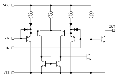
Cautions When Using an Op Amp as a Comparator
Because of the differences above, when the purpose is comparison judgment, selecting a comparator is generally the basic approach. If an op amp is used as a comparator, response can be slower than with a comparator because of phase compensation capacitance and recovery from output saturation.
Also, an op amp is not designed as a logic IC that outputs High/Low signals. The output voltage level, input common-mode voltage range, allowable differential input voltage range, whether the output may swing in the opposite direction from expected, and recovery time must be checked.
If the input changes slowly near the threshold or noise is superimposed on the input, the output may switch unstably. For applications that require hysteresis or high-speed judgment, consider using a comparator as the basic approach. If substituting an op amp, check the datasheet to confirm whether that use is allowed.
Summary of Op Amp Basics
An op amp is an analog IC that amplifies the differential voltage between two input pins and combines this with negative feedback to obtain the required gain and operation. Understanding the pin configuration, internal circuit, and the ideas of high input resistance and low output resistance makes it easier to see why op amps are used for small-signal amplification, buffers, filters, detection circuits, and other applications. During selection, check the power supply configuration, input/output voltage range, gain, offset, slew rate, noise, and temperature conditions according to the application. Op amps and comparators have similar pin configurations, but because their main applications and internal configurations differ, voltage level judgment should be considered with the use of a dedicated comparator in mind.