
Opamps|Basic
Operational Amplifier Gain and Feedback: From Gain Design to Slew Rate
Op Amp Gain and Voltage Gain
To understand op amp amplification, first express how much the output voltage changes relative to the input voltage as gain. Voltage gain, decibel notation, and the difference between open-loop and closed-loop gain provide the foundation for understanding inverting amplifiers, non-inverting amplifiers, and negative feedback.
Defining Op Amp Voltage Gain
In an amplifier circuit using an op amp, voltage gain indicates how much larger the output voltage is than the input voltage. Voltage gain is the output voltage divided by the input voltage. If the input voltage is Vs, the output voltage is Vo, and the voltage gain is Av, it is defined as follows.
\(A_v = \displaystyle\frac{V_o}{V_s}\)
For example, if Av is 10, the output voltage magnitude is 10 times the input voltage magnitude. Defining gain as a voltage ratio also gives a common basis for decibel notation and for comparing open-loop gain with closed-loop gain.
Expressing Voltage Gain in Decibels (dB): AV[dB] = 20 log10(VO/VS)
Op amp voltage gain may range from tens of times to hundreds of thousands of times or more. For this reason, gain is often expressed in decibels (dB) rather than only as a multiplication factor. When voltage gain is expressed in decibels, the common logarithm of the voltage ratio is multiplied by 20. For example, if the open-loop gain of an op amp is 100,000 times (105 times), the decibel value is as follows.
\(20log_{10}(10\,^5) = 100 dB\)
Even a large voltage gain such as an open-loop gain can be compared with fewer digits when it is expressed in dB. For a power ratio, the logarithm is multiplied by 10. For a voltage ratio under the same resistance condition, power is proportional to the square of voltage, so the voltage ratio uses a factor of 20. In other words, a voltage ratio can be considered as 10log10((VoVs)2) = 20log10(VoVs). When an inverting amplifier has a negative voltage gain, the dB value normally represents the magnitude of the gain, while phase inversion is handled separately. The following related units and notations are also useful when reading gain, output amplitude, and frequency response.
(a) dB: A unit that expresses the ratio between two quantities on a logarithmic scale. A factor of 10 is used for power ratios, and a factor of 20 is used for voltage ratios.
\(dB = 10log_{10}(\displaystyle\frac{P_1}{P_2})\)(power ratio)
\(dB = 20log_{10}(\displaystyle\frac{V_1}{V_2})\) (voltage ratio)
(b) Vp-p: Peak-to-peak voltage. It is the difference between the maximum and minimum voltage of a waveform. For a sine wave centered around 0 V and symmetrical above and below the center, Vp-p is twice the peak voltage. Because Vp-p and Vrms have different meanings, conversion should be made only when the waveform type and conditions are known.
(c) Vrms: The RMS value. It is the equivalent DC value that would dissipate the same power as the AC waveform. For a sine wave, it is the peak voltage divided by √2.
\(V_{rms} = \displaystyle\frac{V_p}{√2}\)
(d) dBV: A voltage level referenced to 1 Vrms. 0 dBV represents 1 Vrms.
\(0 dBV = 1V_{rms}\)
(e) dBm: A power level referenced to 1 mW. Converting dBm to voltage requires a load resistance, so the voltage corresponding to 0 dBm differs between 50 Ω and 600 Ω systems.
\(0 dBm = 0.224 V_{rms}\)(with a 50 Ω load)
\(0 dBm = 0.775 V_{rms}\)(with a 600 Ω load)
(f) oct (octave): A unit that represents a frequency span in which the frequency doubles.
-6 dB/oct indicates that the gain decreases by approximately 6 dB each time the frequency doubles.
(g) dec (decade): A unit that represents a frequency span in which the frequency increases by a factor of 10.
-20 dB/dec indicates that the gain decreases by 20 dB each time the frequency increases by a factor of 10.
Since 1 dec is approximately 3.322 oct, -6 dB/oct is treated in practice as almost the same slope as -20 dB/dec.
(h) Basic dB calculation
Because dB values express ratios logarithmically, multiplication and division relationships can be handled as addition and subtraction. Use 20log10 for voltage ratios and 10log10 for power ratios.
\(3dB≈1.41×≈√2\)
\(6dB≈2.00×\)
\(10dB≈3.16×\)
\(20dB≈10×\)
\(16 dB = 10 dB + 6 dB → 3.16 × 2 = 6.32×\)
Difference Between Open-Loop Gain and Closed-Loop Gain
Op amp gain includes open-loop gain, which is the gain without negative feedback, and closed-loop gain, which is the gain of the entire circuit with negative feedback applied. Open-loop gain indicates the capability of the op amp itself. Closed-loop gain is the gain used in an actual amplifier circuit.
Open-loop gain is large, but it changes with product variation, temperature, supply voltage, and frequency. Without negative feedback, even a small input difference can make the output saturate, so open-loop gain cannot be used directly as a stable target gain. Closed-loop gain is the gain of the amplifier circuit including the feedback network. With negative feedback, the gain is easier to set mainly by external components such as resistors rather than by the op amp’s open-loop gain itself. In design work, the required gain is set as closed-loop gain, and open-loop gain and gain-bandwidth product are then checked to see whether that setting is valid over the required frequency range. Inverting and non-inverting amplifiers set closed-loop gain with resistor ratios.
Gain Setting in Inverting and Non-Inverting Amplifiers
In inverting and non-inverting amplifiers, closed-loop gain is mainly determined by the ratio of external resistors.
The gain of an inverting amplifier is expressed as
\(A_v = -\displaystyle\frac{R_f}{R_{in}}\)
The gain of a non-inverting amplifier is expressed as
\(A_v = 1 + \displaystyle\frac{R_f}{R_{in}}\)
Here, Rf is the feedback resistor from the output back to the inverting input. Rin is the resistor from the input signal to the inverting input in an inverting amplifier. Rg is the gain-setting resistor between the inverting input and the reference node in a non-inverting amplifier.
The minus sign in the inverting amplifier equation indicates that the phase of the output signal is inverted relative to the input signal. In a non-inverting amplifier, the input and output signals have the same phase, and the gain is 1 or higher. In practical circuits, the op amp operating range and frequency response must be considered in addition to the gain set by the resistor ratio.
Op Amp Negative Feedback Circuits and Their Effects
An op amp has high open-loop gain, but when used by itself it is affected by gain variation and frequency response. For this reason, op amps are usually used in negative feedback circuits. Negative feedback makes it easier to set closed-loop gain through the feedback factor determined by external components, and it can stabilize gain, extend bandwidth, and reduce distortion or output-side error components. A transfer-function model of negative feedback helps organize these effects along with stability considerations.
Negative Feedback Transfer Function Model
An op amp has high open-loop gain, but it is rarely used as a linear amplifier in open-loop operation. Open-loop gain varies with manufacturing tolerance and temperature, and it decreases as frequency increases. Therefore, open-loop operation makes it difficult to set the desired gain stably and maintain it over the required bandwidth. In typical circuits, part of the output is fed back to the input side, and the feedback factor sets the closed-loop gain. The model below shows an amplifier circuit using negative feedback.

Gain Stabilization, Bandwidth Expansion, and Distortion Reduction by Negative Feedback
Applying negative feedback mainly provides the following advantages in amplifier circuits.
[Advantages of configuring a negative feedback circuit]
- 1. Extends bandwidth
- 2. Reduces the effect of open-loop gain variation on closed-loop gain
- 3. Reduces distortion
1. Extends bandwidth
The change in closed-loop gain and bandwidth caused by negative feedback can be expressed with a transfer function. Let A(s) be the frequency-dependent open-loop gain and β be the feedback factor.
\(G(s) = \displaystyle\frac{V_o(s)}{V_{IN}(s)} = \displaystyle\frac{A(s)}{1 + βA(s)}\)
A(s): frequency-dependent open-loop gain of the op ampβ: feedback factorβA(s): loop gain1+βA(s): factor by which negative feedback reduces closed-loop gain and output-side error components
The open-loop gain of the op amp can be approximated by a first-order lag transfer function. In this approximation, A0 is the low-frequency open-loop gain and ω0 is the pole angular frequency. The relationship between gain reduction and bandwidth expansion due to negative feedback is then expressed as follows.
| A(s) | = | AO | |
| 1 + | ω | ||
| ωO | |||

| VO(s) | = | AO | × | 1 | |
| VIN(s) | 1 + βAO | 1 + | ω | ||
| ωO(1 + βAO) | |||||

The frequency response shown above illustrates the relationship in the equation. If the low-frequency open-loop gain is A0, the closed-loop gain with negative feedback is A01 + βA0, which is smaller than the open-loop gain A0. In the range where the first-order lag approximation is valid, the bandwidth expands approximately from ω0 to ω0(1 + βA0). In other words, negative feedback lowers gain in exchange for widening the frequency range over which the circuit can be used stably.
2. Reduces the effect of open-loop gain variation
The effect of open-loop gain variation on closed-loop gain depends on the loop gain. In the low-frequency range where the loop gain βA0 is sufficiently large, that is, where βA0 >> 1 holds, the gain of the negative feedback circuit can be approximated as 1β. Under this condition, closed-loop gain depends more strongly on the feedback factor set by external components than on the op amp’s open-loop gain itself. Therefore, even if open-loop gain changes somewhat due to temperature characteristics or manufacturing variation, the effect on closed-loop gain is small. For the bandwidth and stability of an inverting amplifier, noise gain rather than signal gain should be used.
\(\displaystyle\frac{V_o}{V_{IN}} = \displaystyle\frac{A_0}{1 + βA_0} = \displaystyle\frac{1}{\displaystyle\frac{1}{A_0} + β} ≈ \displaystyle\frac{1}{β}\)
3. Reduces distortion
The figure below shows a feedback circuit that includes an output-side error component. VD represents an error component generated in the op amp or output stage and corrected within the loop. VD includes distortion components and error voltage that appear at the output. However, input noise and the thermal noise of external resistors are not simply reduced by negative feedback.
[Feedback circuit including distortion and noise]
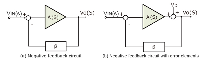
The expression on the right shows the output equation including the error component VD. The component transmitted from VIN to the output is represented by A(s)1 + βA(s), while the VD component is reduced by 11 + βA(s). Therefore, within the frequency range where sufficient loop gain is available, output-side error components inside the loop become smaller.
\(V_o(s) = \displaystyle\frac{A(s)}{1 + βA(s)} × V_{IN}(s) + \displaystyle\frac{1}{1 + βA(s)} × V_D\)
On the other hand, negative feedback circuits have the following considerations. Negative feedback is an effective way to stabilize gain and reduce output-side error components, but it assumes that the op amp operates within its linear operating range and has sufficient phase margin for stable operation.
[Considerations when configuring a negative feedback circuit]
- 1. Closed-loop gain is lower than open-loop gain
- 2. Insufficient phase margin can cause oscillation or ringing
Capacitive load, wiring and PCB parasitics, feedback resistor values, and input capacitance can reduce phase margin. When handling large signals, slew rate, output amplitude range, and load current must be considered in addition to the small-signal bandwidth estimated from GBW.
Negative feedback is a way to handle closed-loop gain, bandwidth, and the influence of error components through feedback factor and loop gain rather than by using the magnitude of open-loop gain directly. Practical circuits are also limited by phase margin, capacitive load, output amplitude, and slew rate. The gain-bandwidth product (GBW) is used as a guideline for estimating small-signal bandwidth.
Gain-Bandwidth Product (GBW)
For a voltage-feedback op amp in the range where the single-pole approximation is valid, the gain-bandwidth product (GBW) is a guideline for estimating the relationship between noise gain (NG) and small-signal bandwidth. If NG is the noise gain and BW is the bandwidth, the relationship can be expressed as follows.
\(GBW ≈ NG × BW\)
or
\(BW ≈ \displaystyle\frac{GBW}{NG}\)
In a non-inverting amplifier, NG is the same as the closed-loop gain. In an inverting amplifier, however, the magnitude of signal gain may not be the same as NG, so bandwidth and stability are estimated using NG. Lower NG corresponds to a wider estimated bandwidth, while higher NG narrows the estimated bandwidth.
The bandwidth calculated from GBW is only a guideline for small-signal frequency response; it is not a guaranteed upper limit under all operating conditions. When output amplitude is large, waveform tracking may be limited by slew rate. Capacitive load and PCB parasitics can also reduce phase margin, so practical circuit design should be judged together with the datasheet, simulation, and bench evaluation.
Op Amp Slew Rate: Large-Signal Speed Limit
An op amp output cannot follow input signal changes without limit. The rate at which the output voltage can change per unit time is expressed as slew rate, and in AC signals it affects the upper limit of output amplitude and frequency. The definition and measurement method of slew rate provide the basis for estimating the slew rate required for sine-wave output and the full-power bandwidth.
Slew Rate Definition and Measurement Circuit
Slew rate is a parameter that indicates how quickly an op amp output voltage can change per unit time. If the output voltage change is ΔV and the time required for that change is Δt, the rate of change is expressed as ΔVΔt. For example, 1 V/µs means that the output voltage can change by 1 V in 1 µs. An ideal op amp would follow a sudden change in the input signal immediately. In an actual op amp, however, the output voltage has a maximum rate of change. When a square-wave pulse with a steep rising or falling edge is applied to the input, the output waveform does not change instantaneously; it changes with a finite slope. The maximum slope of the output voltage is the slew rate. The figure below shows the definition of slew rate.
[Slew-rate measurement circuit and waveform]
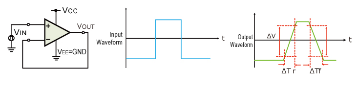
The slew rates for the rising and falling output waveform are calculated from the voltage change and the time required for that change.
\(SR_r = \displaystyle\frac{ΔV}{ΔT_r} \quad SR_f = \displaystyle\frac{ΔV}{ΔT_f}\)
Here, ΔV is the output voltage change, ΔTr is the time required for the rising edge, and ΔTf is the time required for the falling edge. Dividing the output voltage change by the time required for that change gives the slope of the output waveform. This slope is the rising or falling slew rate. When the rising and falling values differ, datasheets may specify the slower value. A signal with a steeper change than this cannot be followed by the output waveform and distortion occurs. Even when an amplifier circuit is configured, slew rate is fundamentally unchanged because it is the rate of output change.
Op amps are used to amplify both DC and AC signals. They have finite response speed, so they cannot handle every type of signal. In the voltage follower configuration shown above, a DC input voltage is limited by the input voltage range and output voltage range. For AC signals with frequency content, gain-bandwidth product and slew rate constraints are added.
For sine-wave output, the relationship among slew rate, amplitude, and frequency can be used to estimate the range in which the output waveform can follow the input.
Slew Rate Required for Sine-Wave Output
When outputting a sine wave, the required slew rate is determined by the waveform amplitude and frequency. As amplitude or frequency increases, the output voltage changes more steeply. If slew rate is insufficient, waveform distortion occurs. The maximum slope of the output waveform can be obtained from the sine-wave equation, which gives the required slew rate. If the slew rate of the op amp is known, the same relationship can also be used to calculate the upper limit of output frequency or amplitude.
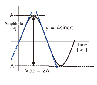
Consider the sine-wave output shown above. The output voltage of the sine wave is expressed as follows.
\(y = A\ sin(ωt)\)
Here, A is the peak amplitude of the sine wave and ω is the angular frequency. To obtain the slope of the output voltage, differentiate this equation with respect to time t.
\(\displaystyle\frac{dy}{dt} = Aω\ cos(ωt)\)
The slope of a sine wave is maximum when cos(ωt) = 1. Therefore, the maximum slope of the output waveform is as follows.
\(SR = Aω = 2πfA\)
This equation represents the slew rate required for a sine wave with a specified peak amplitude A and frequency f. Conversely, if the op amp slew rate SR is known, solving the same equation for f gives the maximum frequency that can be output at that amplitude.
\(f = \displaystyle\frac{SR}{2πA}\)
If the peak-to-peak voltage of the sine wave is VPP, then VPP = 2A. Substituting A = VPP2 into the equation gives the following relationship.
\(f = \displaystyle\frac{SR}{πV_{PP}}\)
Solving the same relationship for VPP also gives an estimate of the peak-to-peak voltage that can be output at a specified frequency f.
\(V_{PP} = \displaystyle\frac{SR}{πf}\)
Design Judgment Using Full-Power Bandwidth
Full-power bandwidth is a guideline for the frequency range in which a sine wave with a specified output amplitude can be output with little waveform distortion caused by slew-rate limiting. Using the equation f = SRπVPP, the upper frequency limit can be estimated for the desired output amplitude VPP. This bandwidth is not the small-signal bandwidth measured from frequency response or estimated from GBW; it is determined by large-signal slew-rate limitation.
For example, consider an op amp with SR=1V/µs outputting a 1VPP sine wave. This example estimates the allowable frequency from slew rate when the required output amplitude is known. Although 1VPP corresponds to a peak amplitude of A=0.5V, the previously derived equation f = SRπVPP allows VPP to be substituted directly. The calculation conditions are SR = 1×10⁶ V/s and VPP=1V.
\(f = \displaystyle\frac{SR}{πV_{PP}} = \displaystyle\frac{1×10\,^6}{π×1} = 318.4 kHz\)
This result shows that, for a 1VPP sine wave, approximately 318kHz is the upper frequency guideline based on slew rate. If the required frequency approaches or exceeds this value, the op amp may not be able to follow the slope of the output waveform, and the sine wave is likely to become distorted. When slew-rate limiting becomes strong, the output waveform includes linear changes and approaches a triangular waveform.
During design, first determine the required output amplitude and frequency, then provide sufficient margin against the full-power bandwidth under those conditions. If the margin is small, select an op amp with a higher slew rate, reduce the output amplitude, or reconsider the frequency range to be handled. In actual selection, also consider the closed-loop bandwidth estimated from GBW, output amplitude range, load conditions, allowable distortion, and datasheet test conditions.
Summary of Op Amp Amplification and Feedback
When designing op amp amplification, first determine the required closed-loop gain for the inverting or non-inverting amplifier, then set that gain with resistor ratios. The key point is to obtain stable gain through negative feedback rather than by using open-loop gain directly. Negative feedback is related to improvements in gain accuracy, bandwidth, and distortion, but higher closed-loop gain narrows the usable frequency range through GBW. Large-amplitude signals also require checks of slew rate and full-power bandwidth. Considering gain, bandwidth, and signal amplitude together helps estimate whether the op amp can operate appropriately for the application.