
Opamps|Basic
What Are Operational Amplifier Input Characteristics? Input Accuracy and Absolute Maximum Ratings
To use an op amp correctly, it is important to separate input-signal accuracy from the voltage and current conditions that protect the IC from damage. Input offset voltage is a source of output error, while supply voltage, differential input voltage, common-mode input voltage, and input current under out-of-rating input conditions are items used to judge the safe limits shown in the datasheet.
This article explains op amp input characteristics by dividing them into input accuracy and safety ratings. It covers the meaning of input offset voltage and its effect on output error, the difference between absolute maximum ratings and operating conditions, how to read differential and common-mode input voltage ratings, and how to limit input current when an input pin is driven outside the rated range.
Absolute maximum ratings and operating conditions do not have the same meaning. In the following sections, they are checked separately.
What Are Op Amp Input Characteristics?
Op amp input characteristics can be divided into two broad groups. The first group describes how accurately the input signal can be handled. The second group describes the upper limits of the voltage and current that may be applied to the input pins and supply pins.
Input bias current is a small current that flows at the input pins during normal operation. When it is combined with source resistance, it can become a source of voltage error. Supply voltage, differential input voltage, common-mode input voltage, and input current under out-of-rating input conditions, on the other hand, are checked to avoid IC degradation or damage.
| Category | Item | What to check | Design meaning |
|---|---|---|---|
| Input accuracy | Input offset voltage | Error voltage referred to the input terminals | Estimate output error |
| Input accuracy | Input bias current | Small current flowing into the input pins during normal operation | Estimate voltage error with high source resistance |
| Safety ratings | Supply voltage | Potential difference between the VCC and VEE pins | Avoid overvoltage between supply pins |
| Safety ratings | Differential input voltage | Voltage difference between the +input and -input pins | Avoid overstress on the input stage or input-to-input protection device |
| Safety ratings | Common-mode input voltage | Relationship between input pin potential and supply pin potential | Check the allowable input pin potential |
| Safety ratings | Input current under out-of-rating input conditions | Current flowing through protection devices when an out-of-rating voltage is applied | Avoid degradation or damage to protection devices or the input stage |
Characteristics Affecting Input Accuracy
Parameters related to input accuracy during normal operation include input offset voltage and input bias current. Input offset voltage is an error voltage referred to the input terminals. Input bias current is a small current that, together with source resistance, can create a voltage error. Both parameters can affect output error in circuits that handle very small sensor signals or require high DC accuracy.
What Is Input Offset Voltage?
In an ideal op amp, if the potential difference between the +input pin and -input pin is 0 V, the output would ideally be 0 V. In an actual op amp, however, device mismatch and other input-stage variations can cause the output to shift even when the differential input voltage is 0 V. The correction voltage that must be applied between the input terminals to bring this output shift to 0 V is called the input offset voltage.
Input offset voltage is normally expressed in mV or µV. A value closer to 0 is more ideal, and the parameter is especially important in circuits that require high DC accuracy.

Outside the common-mode input range, input offset voltage may increase rapidly, and the op amp may no longer operate properly as an amplifier. When evaluating input offset voltage, also check the measurement conditions and the input common-mode voltage range.
Why Values Are Expressed as Input-Referred
An input-referred value expresses an error that appears at the output as an equivalent voltage at the input. Because closed-loop gain and noise gain change depending on the circuit configuration, it is difficult to compare IC error or circuit-to-circuit error by looking only at the output-side value. Expressing the error at the input makes it easier to convert it to output error under the actual circuit conditions and to read datasheet values such as input offset voltage and input-referred noise on the same basis.
An input-referred value is not the actual output error itself. The error that appears at the output is estimated by multiplying the input-referred value by the circuit closed-loop gain or noise gain. Therefore, check the datasheet value given at the input side, and then evaluate it in the actual circuit together with gain conditions, source resistance, temperature, and bandwidth.
How Input Offset Voltage Affects Output Error
As a first estimate, the output error caused by input offset voltage can be calculated by multiplying the input offset voltage by the noise gain.
\(V_{OUT\_error}≈V_{OS}×noise\ gain\)
VOS is the input offset voltage. Noise gain is the gain by which input-referred error appears at the output.
In a non-inverting amplifier where the noise gain is the same as the closed-loop gain, the estimate can be expressed as follows.
\(V_{OUT\_error}≈V_{OS}×\left(1+\displaystyle\frac{R_F}{R_G}\right)\)
RF is the feedback resistor, and RG is the gain-setting resistor. In an inverting amplifier as well, output error caused by input offset voltage should be considered using noise gain, not signal gain. For example, when RF/RG = 100, the signal gain of the inverting amplifier is -100, but the noise gain for input offset voltage is 1 + RF/RG = 101.
Therefore, if input offset voltage VOS = 1 mV and the noise gain is 101, the output error is approximately 101 mV. Even a small input-referred error can appear as a large output-side error in a circuit with high noise gain.
Input Offset Voltage Variation and Normal Distribution
When the values of individual devices are observed, input offset voltage tends to be distributed in both the positive and negative directions around 0 V. In many datasheets, the specified value is shown as the maximum absolute value of VOS, so actual devices may have either positive or negative offset.
The distribution can sometimes be approximated as a normal distribution, but it depends on the product and measurement conditions. For design, it is more important to include the maximum value and temperature drift in the design margin than to rely on the detailed shape of the distribution. For high-accuracy DC amplification or sensor-signal amplification, check not only the datasheet maximum value but also the temperature drift.
Even when the distribution appears close to a normal distribution, do not relax the design margin based only on the center value. Treat the datasheet maximum value as the guaranteed limit, and check whether the output error remains within the allowable range for either positive or negative offset.
Input Offset Voltage Temperature Drift
Input offset voltage changes with temperature. This change is called input offset voltage drift, or offset voltage temperature drift. It is generally expressed in µV/°C and becomes an important item in applications with a wide temperature range or very small signals.
\(ΔV_{OS}≈drift×ΔT\)
Drift is the input offset voltage drift, and ΔT is the temperature change. Treat this as an error factor separate from the initial VOS.
For example, if input offset voltage drift is 1 µV/°C and the temperature change is 50°C, the temperature-related input-referred error is approximately 50 µV. Multiplying this value by the circuit noise gain gives an estimate of the output error caused by temperature change.
What Is Input Bias Current?
Input bias current is a small current that flows into the op amp input pins during normal operation. It is different in both occurrence condition and design treatment from the input current that flows through protection devices when an input pin voltage is outside the rated range. Input bias current is not a protective current used to avoid damage; it is an error factor that affects input accuracy.
In circuits with large source resistance or feedback resistance, input bias current causes a voltage drop across the resistance and appears as an input-referred error. In the datasheet, check the typical and maximum values of input bias current, the temperature conditions, and the resistance values used in the actual circuit.
How Input Bias Current Affects Input Error
The input-referred error caused by input bias current can be estimated from the product of input bias current and source resistance.
\(V_{error}≈I_B×R_S\)
IB is the input bias current, and RS is the source resistance. Treat this as an error factor separate from input offset voltage.
For example, if input bias current IB = 100 nA and source resistance RS = 10 kΩ, the input-referred error is approximately 1 mV. In circuits with high source resistance, error caused by input bias current may not be negligible, even when the input offset voltage is small.
How to Read Absolute Maximum Ratings
Next, check the difference between ratings that prevent op amp damage and conditions that confirm normal operation. When checking supply voltage and input pin voltage, it is important to read limiting values and operating-guarantee conditions separately.
What Are Absolute Maximum Ratings?
Absolute maximum ratings are limiting values that must not be exceeded. They are not conditions that guarantee normal operation. Even a momentary excursion beyond an absolute maximum rating can lead to IC characteristic degradation or damage. Operation and electrical characteristics are not guaranteed merely because the condition is within the absolute maximum rating; the design operating point must be checked using the recommended operating conditions and electrical characteristics conditions.
Around the op amp input pins, not only supply voltage but also differential input voltage, common-mode input voltage, and input current under out-of-rating input conditions are items to check in the absolute maximum ratings. In design, first confirm that the circuit stays within the recommended operating conditions. Then check whether the absolute maximum ratings are exceeded under worst-case conditions such as power-up, transient input, or external overvoltage.
For this reason, absolute maximum ratings should be treated as boundaries that must not be crossed even during abnormal or transient conditions, not as design targets. Even if two values look similar, their meanings differ depending on the datasheet table in which they appear.
Difference Between Absolute Maximum Ratings and Operating Conditions
Datasheets list absolute maximum ratings, recommended operating conditions or operating supply voltage range, and electrical characteristics conditions separately. These items may look similar, but their meanings are different.
| Item | Meaning | If exceeded | Normal operation guarantee |
|---|---|---|---|
| Absolute maximum ratings | Limiting values for avoiding damage or degradation | May cause characteristic degradation or damage | Not guaranteed |
| Recommended operating conditions / operating supply voltage range | Range used for normal operation | May not operate according to specifications | Check operation within this range |
| Electrical characteristics conditions | Conditions for measuring or guaranteeing electrical characteristics | Electrical characteristics table values may not apply directly | Read the characteristics table under these conditions |
Supply Voltage and Operating Supply Voltage Range
The supply voltage in the absolute maximum ratings is checked as the potential difference between the VCC and VEE pins. The key point is to check the difference between the positive and negative supplies, not the VCC voltage alone.
\(V_{CC}-V_{EE}≤absolute\ maximum\ rated\ supply\ voltage\)
This formula is a limit check for avoiding damage or degradation. It does not guarantee normal operation.
For normal operation, the device must be used within the operating supply voltage range. Depending on the product, the maximum value of the absolute maximum rated supply voltage and the maximum value of the operating supply voltage range may be the same, but their meanings are different.
\(lower\ limit\ of\ operating\ supply\ voltage\ range≤V_{CC}-V_{EE}≤upper\ limit\ of\ operating\ supply voltage\ range\)

For example, when VCC = 24 V and VEE = -12 V are applied to a product with an absolute maximum rated supply voltage of 36 V, the potential difference between the supply pins is 36 V. However, whether the device operates according to specifications under this condition must be checked separately using the operating supply voltage range and electrical characteristics conditions.
Input-Related Ratings to Check in the Datasheet
When applying input characteristics to circuit design, do not judge from a single rating alone. Check supply, input-pin, and input-current items together. Because values differ by product, the final judgment must follow the target product datasheet.
| Datasheet item | What to check | What can happen if missed |
|---|---|---|
| Supply voltage | Whether VCC – VEE exceeds the absolute maximum rating | Degradation or damage due to overvoltage between supply pins |
| Operating supply voltage range | Whether the supply is within the range for specified operation | Operation or characteristics may fall outside guaranteed conditions |
| Differential input voltage | Whether the voltage difference between +input and -input is within the rating | Excessive stress on the input stage or input-to-input protection device |
| Common-mode input voltage | Whether input pin potential is within the allowable range relative to the supply pins | Conduction of protection devices or abnormal input-stage operation |
| Input current under out-of-rating input conditions | Whether current through protection devices is below the allowed value | Degradation or damage to protection devices or the input stage |
Absolute maximum ratings are limiting values for avoiding damage or degradation. Whether the actual circuit operates according to specifications must be checked under the conditions listed in the operating conditions and electrical characteristics sections.
Differential Input Voltage
Differential input voltage is the voltage difference applied between the +input pin and -input pin. During normal negative-feedback operation, the voltage difference between the input pins is small, but a large difference can occur during startup or abnormal input conditions. Check that the rating is not exceeded.
What Is Differential Input Voltage?
Differential input voltage is the voltage difference between the +input pin and -input pin. It can be defined as follows.
\(V_{ID}=V_{IN+}-V_{IN-}\)
VIN+ is the non-inverting input pin voltage, and VIN– is the inverting input pin voltage.
When checking the differential input voltage rating, in many cases the absolute value of the voltage between the input pins must not exceed the specified value. Because datasheet notation differs by product, follow the notation in the target datasheet.
\(|V_{ID} |≤absolute\ maximum\ rating\ for\ differential\ input\ voltage\)
| Item | Voltage checked | Relationship being checked | Main purpose |
|---|---|---|---|
| Differential input voltage | Difference between the +input and -input pins | Relationship between input pins | Avoid applying excessive voltage difference to the input stage or input-to-input protection device |
| Common-mode input voltage | Input pin potential | Relationship between input pins and supply pins | Keep input pin potential within the allowable range |
Relationship Between Input Pin Voltage Conditions and Input Current
Input-pin safety ratings cannot be judged from the voltage difference between the input pins alone. First, check whether the difference between the +input and -input pins is within the differential input voltage rating. Next, check whether each input pin potential is within the allowable common-mode input voltage range relative to the VCC and VEE pins. If these conditions are not met, current may flow through input protection devices, an input-to-input clamp, or toward a supply pin.
In other words, differential input voltage checks the relationship between the input pins, common-mode input voltage checks the relationship between the input pins and the supply pins, and input current under out-of-rating input conditions checks the current that flows through protection paths when these conditions are exceeded. Even if the potential difference between the +input and -input pins is small, the safety ratings are not necessarily satisfied if both input pins are outside the allowable range relative to the supply pins.
During design, combine the signal source output range, supply voltage, and startup or shutdown states, and check each input pin potential and the voltage between the input pins under worst-case conditions. This reduces the risk of overlooking differential input voltage, common-mode input voltage, or current flowing through protection devices.
How ESD Protection Devices Determine Differential Input Voltage Limits
ICs include ESD protection devices. The input pin protection device may be connected only to the VEE side, or it may be connected to both the VCC and VEE sides. If a protection device is also present on the VCC side, the input pin potential is limited by the VCC-side condition as well.
| Protection device configuration | Main input-pin limit | What to check |
|---|---|---|
| VEE side only | Pay attention to overvoltage toward the VEE side | Input transistor withstand voltage and product-specific differential input voltage rating |
| Both VCC and VEE sides | Pay attention to both the VCC and VEE sides | Whether the input pin is within the allowable range relative to the supply pins |

When Clamp Diodes Are Connected Between Input Pins
In products that include clamp diodes between the input pins, a large voltage difference between the +input and -input pins causes the diode to conduct and suppress the voltage difference between the pins. Therefore, the differential input voltage rating may be limited to several volts, or to a value close to the diode forward voltage. The specific value and conditions differ by product, so check the target product datasheet.
However, when a clamp diode conducts, check not only the voltage between the input pins but also the clamp current flowing between the +input and -input pins. If the datasheet shows an input current, clamp current, injection current, or a current limit in a note, include source impedance and series resistance so that the current does not exceed that value. Even when the voltage appears to be within the rating, avoid conditions where the current in the clamp path exceeds the allowable value.

Common-Mode Input Voltage
Common-mode input voltage is the item used to check the range of input pin potential relative to the supply pins. Differential input voltage checks the difference between input pins, while common-mode input voltage checks the relationship between input pin potential and the supply voltage. Read it separately from the normal operating range.
What Is Common-Mode Input Voltage?
Common-mode input voltage is the input pin potential when the potentials of the +input and -input pins are viewed relative to the supply pins. It is sometimes expressed as the average voltage of the two input pins.
\(V_{ICM}=\displaystyle\frac{V_{IN+}+V_{IN-}}{2}\)
VICM is the common-mode input voltage. The exact treatment when a differential signal is present depends on the circuit conditions.
Even when VICM is checked as an average voltage, also confirm that each of the +input and -input pins is within the allowable potential range. When a differential signal is superimposed, VICM may be within the range while only one input pin approaches the upper or lower limit.
In datasheets, common-mode input voltage may be listed in both the absolute maximum ratings section and the electrical characteristics or recommended operating conditions section. Read the limit check for avoiding damage or degradation separately from the range used to confirm normal operation and guaranteed characteristics.
Difference Between Common-Mode Input Voltage and Common-Mode Input Voltage Range
The common-mode input voltage in the absolute maximum ratings and the common-mode input voltage range in the electrical characteristics have different purposes. The former is a limit for avoiding damage or degradation. The latter is the range used to confirm normal operation.
| Item | Meaning | Use |
|---|---|---|
| Common-mode input voltage in the absolute maximum ratings | Limit for avoiding damage or degradation when voltage is applied to the input pins | Check conditions that must not be exceeded |
| Common-mode input voltage range in the electrical characteristics | Input common-mode range in which the op amp operates according to specifications | Check normal operation and guaranteed characteristics |
Common-Mode Input Voltage Limits Shown as VEE – 0.3 V to VCC + 0.3 V
In the absolute maximum ratings, common-mode input voltage may be shown as a limit such as VEE – 0.3 V to VCC + 0.3 V. This notation indicates how far the input pin potential is allowed to move relative to the supply pins.
This value is a representative margin, not a fixed conduction threshold for the protection device. If the input pin potential moves outside this range, current may flow through input protection devices or parasitic elements, which can lead to degradation or damage.
The actual upper and lower limits, allowable input current, and protection circuit configuration differ by product. During design, also check the common-mode input voltage range in the electrical characteristics and any injection-current conditions.

How Input Range Differs Depending on Protection Devices
In products without a protection device on the VCC side, common-mode input voltage may not be directly limited by the VCC voltage and may instead be determined by another withstand-voltage condition. For this reason, common-mode input voltage depends on the input pin protection circuit configuration, parasitic elements, input transistor withstand voltage, and other factors. Always check the target product datasheet.
Input Current and Protection Circuits During Out-of-Rating Input Conditions
The input current discussed in this section is not the input bias current that flows in the input stage during normal operation. It is the current that flows through protection devices or clamp paths when an out-of-rating voltage is applied to an input pin. If this current becomes large, it may degrade or damage the protection device, input stage, or surrounding circuit. Therefore, when an out-of-rating input condition is expected, check the allowable input current in the datasheet, the current path, and limiting methods using external diodes or a series resistor.
What Is Input Current During Out-of-Rating Input Conditions?
Input current during out-of-rating input conditions is the current that flows into or out of an input pin when the input pin voltage is outside the allowable range for differential input voltage or common-mode input voltage. It differs from input bias current during normal operation in both occurrence condition and check purpose. Depending on the product, datasheets may use terms such as input current, clamp current, or injection current, so check not only the item name but also the measurement conditions, notes, and current direction.
When checking input current, also confirm whether the current flows into the input pin or out of the input pin. Depending on the product, the current direction and magnitude may change with input voltage polarity, power-supply state, and protection structure. For protection resistor design, prioritize the notes and allowable input current in the target product datasheet.
Current Paths When an Out-of-Rating Voltage Is Applied to an Input Pin
If the input pin voltage is lower than VEE – 0.3 V or higher than VCC + 0.3 V, or otherwise exceeds the allowable range, current may flow through input protection devices toward a supply pin or between input pins. If this current becomes large, it can cause degradation or damage to the protection device or input stage. Because the 0.3 V value and current path depend on the product protection structure, check the absolute maximum ratings, notes, and input-current limiting conditions for the target product.
The current path changes depending on which side the input pin voltage exceeds. For positive overvoltage, current may flow toward the VCC side. For negative overvoltage, current may flow toward the VEE side or a reference potential. However, because the protection device configuration differs by product, do not generalize the current path. Follow the pin conditions and notes in the datasheet.
Even if a protection device conducts, the power line or surrounding circuit may not be able to safely absorb the current. When the power supply is off, or when the power-line impedance is high, current from the input pin may raise the supply voltage. If an out-of-rating input condition is expected, also check where the current flows and what return path it uses.
Limiting Input Voltage with Clamp Diodes
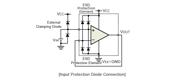
In circuits where an out-of-rating voltage may be applied to an input pin, consider limiting the voltage outside the input pin instead of relying only on internal protection devices. A representative method is to add external clamp diodes between the input pin and the supply lines. If the diode conducts first during overvoltage, current flows from the input pin toward the VCC or VEE side, limiting the input pin voltage to approximately VCC + VF or VEE – VF.
The figure example shows the concept of adding clamp diodes outside the op amp input pin, routing positive overvoltage toward the VCC side and negative overvoltage toward the VEE side. It is not a figure of an internal structure common to all products. It is an example of an external circuit used to reduce the current burden on internal protection devices during overvoltage.
The advantage of external clamp diodes is that they provide an additional current path during overvoltage. However, if the supply line used as the clamp destination cannot absorb the current, the current flowing from the input pin may raise the supply voltage. Check the diode forward voltage, allowable current, and return path for clamp current together with the target product datasheet and the surrounding circuit conditions.
In high-impedance input circuits or circuits handling very small signals, leakage current and capacitance of the external diode may affect input error, bandwidth, or response speed. A clamp diode limits input pin overvoltage, but it does not necessarily limit the clamp current by itself. Therefore, as described next, combine it with a series resistor and keep the current through the diode or protection device below the allowable value.
Limiting Input Current with a Resistor and Calculating Resistance
If an out-of-rating voltage may be applied to an input pin, place a series resistor before the input pin to keep the current flowing through the protection device below the allowable value in the datasheet. In the figure example, a series resistor is placed between the signal source and the op amp input pin, and the resistor limits the current flowing toward the protection device during overvoltage. The series resistor does not remove the overvoltage itself; it limits the current that flows after clamping.
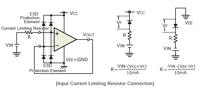
When calculating the resistance value, first consider the voltage applied across the series resistor during overvoltage. For positive overvoltage, the input pin voltage is clamped near VCC + VF, so the voltage across the series resistor is the maximum expected input voltage minus that clamp voltage. Choose the resistance value so that this voltage produces no more than the allowable input current for the target product.
\(R_{IN}≥\displaystyle\frac{V_{IN\_MAX}-(V_{CC}+V_F)}{I_{IN\_MAX}}\)
VIN_MAX is the maximum expected input voltage, VF is the forward voltage of the protection device, and IIN_MAX is the allowable input current. If the numerator is 0 or negative, treat the condition as one in which no positive-side clamp current flows under that condition; do not treat it as a negative resistance value.
For negative overvoltage, limit the amount by which the input pin voltage falls below VEE – VF using the series resistor. Because the amount of negative overvoltage is handled as a positive voltage difference, first confirm whether the input voltage exceeds on the positive side or negative side.
\(R_{IN}≥\displaystyle\frac{(V_{EE}-V_F)-V_{IN\_MIN}}{I_{IN\_MAX}}\)
VIN_MIN is the minimum expected input voltage. If the sign is handled incorrectly, the resistance estimate can be greatly wrong, so confirm the current direction and clamp destination before substituting values into the formula.
For example, consider a circuit in which VCC = 5 V, VF = 0.6 V, and the input pin may be driven up to 12 V. As an example condition, assume that the input current should be limited to 10 mA or less. In positive overvoltage, the voltage across the series resistor is 12 V – (5 V + 0.6 V) = 6.4 V, so the required resistance is RIN ≥ 6.4 V / 0.01 A = 640 Ω.
The value 10 mA is a condition used in this calculation example. It is not an allowable value that can be applied to op amps in general. In actual design, prioritize the allowable input current stated in the target product datasheet, and select a standard resistor value larger than the calculated value. Also check resistor tolerance, temperature, resistor power rating, the time constant with input capacitance, and the effect on signal accuracy.
Increasing the series resistance reduces input current under out-of-rating input conditions. During normal operation, however, it is similar to increasing the source resistance, and it can increase error caused by input bias current, thermal noise, and the time constant with input capacitance. Do not judge only from input-current limiting. Check both protection and signal accuracy, and choose a resistance value that still satisfies the required response speed.
Summary
When checking op amp input characteristics, separate input-accuracy items from rating items used to avoid damage or degradation. Input offset voltage affects output error, and input bias current becomes an error factor in combination with source resistance. Supply voltage, differential input voltage, common-mode input voltage, and input current under out-of-rating input conditions must be checked so that absolute maximum ratings and operating conditions are not exceeded. In the final design, always confirm the absolute maximum ratings, operating conditions, and electrical characteristics in the target product datasheet.
Related topics to check include basic op amp operation, amplification and feedback, and op amp product lists. Confirm the actual URLs before publication and set them as related links in the article body.
【Download Documents】 Thermal Design of Semiconductor Components in Electronics
Thermal design has become a new issue in the design of electronic equipment in recent years, as thermal countermeasures have been the focus of attention. Although heat has been an important consideration for some time, the requirements for electronic equipment have changed in recent years, making it necessary to review conventional thermal countermeasures. This handbook describes thermal design based on the assumption that ICs and transistors are basically used in electronic equipment.
