AC-DC|Design
Design Example Circuit
2018.07.26
Points of this article
・A self-excitation type flyback converter using a quasi-resonant design utilizes the voltage resonance between the transformer primary winding inductor and a resonance capacitor.
・The quasi-resonant design makes possible reduced switching loss and noise levels.
In the previous section, we explained power supply ICs used in design. This time, we will describe a design example circuit.
Quasi-Resonant Design
As explained the last time, the power supply IC used is the BD7682FJ-LB, an AC-DC converter controller IC used for SiC MOSFET driving. The conversion circuit uses a quasi-resonant design, in a self-excitation type flyback converter that uses the voltage resonance of the transformer primary winding inductor and a resonance capacitor. In general, such circuits make possible lower loss and noise levels compared with PWM flyback converters.
The circuit is in essence a flyback converter, and so energy accumulated in the transformer during MOSFET on-time is transmitted to the secondary side during MOSFET off-time. This operation is the same as in a PWM flyback converter, but in a quasi-resonant design, after the transformer has discharged energy, voltage oscillations occur due to resonance between the transformer primary winding inductor and the capacitance of a resonance capacitor. These voltage oscillations are used to cause the IC to detect the Vds bottom voltage and turn on the next cycle. When turn-on occurs with this timing, the current flowing in the transformer is zero and the drain voltage is also low, and so switching losses and noise can be reduced. These are advantages offered by the quasi-resonant design.
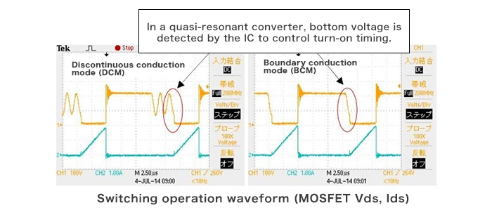
It should be noted that switching losses in a quasi-resonant converter operating in this manner are dominated by losses during MOSFET off-time, and essentially no losses occur during MOSFET on-time.
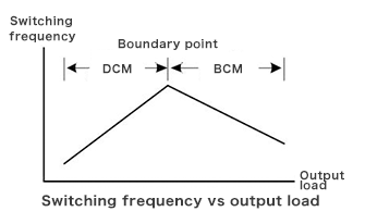
Another feature of this operation is that under light loading, operation becomes discontinuous, and the switching frequency rises as the load is increased. Thereafter, boundary conduction mode operation occurs at a certain load current (boundary point), and in this state the switching frequency declines with increasing load. Thus the switching frequency changes with the load, and so this device can be called one kind of PFM converter.
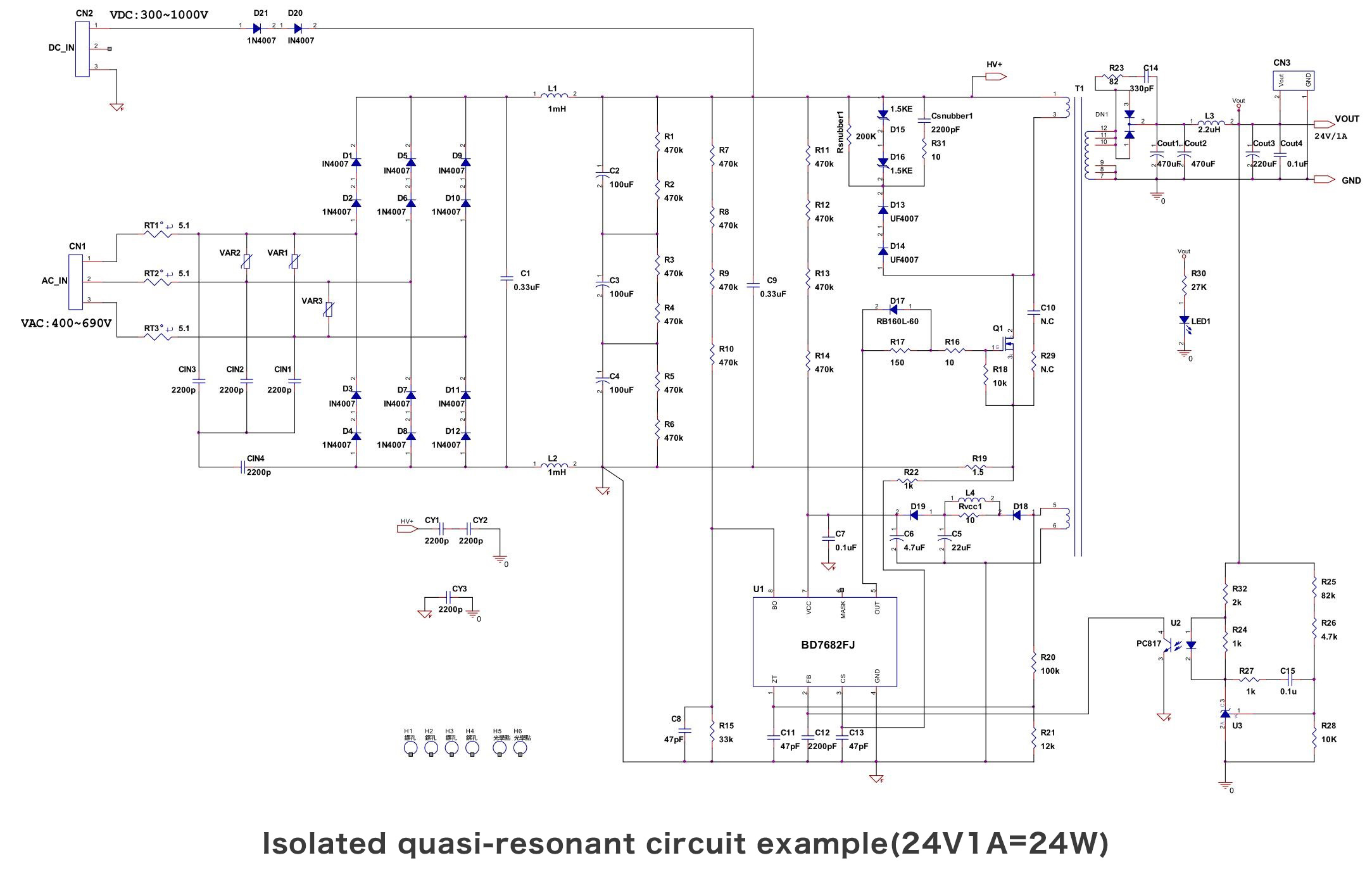
Design Example of 24V/1A Isolated Quasi-Resonant Converter
The input/output conditions and circuit diagram for the design example are shown below. Based on these conditions, we calculate the values of the circuit components.
Output: 24V, 1A(24W)
Input: 300 to 900VDC(400 to 690VAC)
With respect to the input, both a DC voltage input and an AC voltage input are provided, but after rectification, the AC input voltage becomes a DC voltage, and so component values are set assuming a DC input voltage value.
Click on the circuit diagram to enlarge it.
AC-DC
Basic
- AC-DC Basics
- DC-DC Conversion (Regulated) System after Smoothing
- Design Procedure for AC-DC Conversion Circuits (Overview)
- Issues and considerations in AC-DC Conversion Circuit Design
- Summary
- Extra Plus Basic Knowledge
Design
-
Overview of Design Method of PWM AC-DC Flyback Converters
- Isolated Flyback Converter Basics: Flyback Converter Operation and Snubber
- Isolated Flyback Converter Basics: What are Discontinuous Mode and Continuous Mode?
- Want are Isolated Flyhback Convertors?
- Design Procedure
- Isolated Flyback Converter Basics: What is Switching AC-DC Conversion?
- Determining Power Supply Specifications
- Designing Isolated Flyback Converter Circuits
- Isolated Flyback Converter Basics: What are Characteristics of Flyback Converter?
- Designing Isolated Flyback Converter Circuits: Transformer Design (Calculating numerical values)
- Choosing an IC for Design
- Designing Isolated Flyback Converter Circuits: Transformer Design (Structural Design) – 1
- Designing Isolated Flyback Converter Circuits: Transformer Design (Structural Design) – 2
- Designing Isolated Flyback Converter Circuits: Selecting Critical Components ? MOSFET related – 1
- Designing Isolated Flyback Converter Circuits: Selecting Critical Components ? MOSFET related – 2
- Designing Isolated Flyback Converter Circuits: Selecting Critical Components ? CIN and Snubber
- Designing Isolated Flyback Converter Circuits: Selecting Critical Components ? Output Rectifier and Cout
- Designing Isolated Flyback Converter Circuits: Selecting Critical Components ? VCC of IC
- Designing Isolated Flyback Converter Circuits: Selecting Critical Components – IC Settings Etc.
- Designing Isolated Flyback Converter Circuits: Addressing EMI and Output Noise
- Example Board Layout
- Summary
-
Overview of Design Examples of AC-DC Non-isolated Buck Converters
- What are Buck Converters? – Basic Operation and Discontinuous Mode vs. Continuous Mode
- Selection of Power Supply ICs and Design Examples
- Selecting Critical Components: Input Capacitor C1 and VCC Capacitor C2
- Selecting Critical Components: Inductor L1
- Selecting Critical Components: Current Sense Resistor R1
- Selecting Critical Components: Output Capacitor C5
- Selecting Critical Components: Output Rectifying Diode D4
- EMI Countermeasures
- Board Layout and Summary
-
Introduction
- Design Procedure
- IC Used in Design
- Power Supply Specifications and Replacement Circuit
- Synchronous Rectifying Circuit Section: Selection of Synchronous Rectifying MOSFET
- Synchronous Rectification Circuit Section: Power Supply IC Selection
- Troubleshooting ①: Case When Secondary-Side MOSFET Suddenly Turns OFF
- Synchronous Rectification Circuit Section: Selection of Peripheral Circuit Components-C1, R3 at MAX_TON Pin, and VCC Pin
- Troubleshooting ②: Case When Secondary-Side MOSFET Turns On Due to Resonance Under Light Loading
- Troubleshooting ③: Case When, Due to Surge, VDS2 Rises to Above Secondary-Side MOSFET VDS Voltage
- Comparison of Efficiency of Diode Rectification and Synchronous Rectification
- Points to Note Relating to PCB Layout
- Summary
- Synchronous Rectification Circuit Section: Selection of Peripheral Circuit Components-D1, R1, R2 at DRAIN Pin
- Shunt Regulator Circuit Section: Selection of Peripheral Circuit Components
-
Introduction
- Power Supply ICs Used in Design: Optimized for SiC MOSFETs
- Design Example Circuit
- Transformer T1 Design – 1
- Transformer T1 Design – 2
- Selecting Critical Components: MOSFET Q1
- Selecting Critical Components: Input Capacitor and Balancing Resistor
- Selecting Critical Components: Switch Setting Resistors for Overload Protection Points
- Selecting Critical Components: VCC-Related Components of Power Supply ICs
- Selecting Critical Components: Components Related to Power Supply IC BO (Brownout) Pins
- Selecting Critical Components: Components Related to Snubber Circuits
- Selecting Critical Components: MOSFET Gate Drive Adjustment Circuit
- Selecting Critical Components: Output Rectifying Diode
- Selecting Critical Components: Output Capacitors, Output Setting and Control Components
- Selecting Critical Components: Current Sense Resistors and Components Related to Detection Pins
- Selecting Critical Components: Components for Dealing with EMI and Output Noise
- PCB Layout Example
- Example Circuit and Component List
- Evaluation Results: Efficiency and Switching Waveform
- Summary
Evaluation
-
What are Isolated Flyback Converters Performance Evaluation and Checkpoints?
- Overview and important features of a power supply IC used in example performance evaluation
- Design goals and circuits in performance evaluation
- Performance evaluation using an evaluation board: Measurement method and results
- Critical checkpoint: Output transient response and rising output voltage waveform
- Critical checkpoint: Measuring temperature and loss
- Critical checkpoint: Aluminum electrolytic capacitors
- Summary
- Critical checkpoint: Transformer saturation
- Critical checkpoint: MOSFET VDS and IDS, and rated voltage of output rectifier diode
- Critical checkpoint: Vcc voltage
Product Information
FAQ