AC-DC|Design
Shunt Regulator Circuit Section: Selection of Peripheral Circuit Components
2020.03.25
Points of this article
・The output voltage is set by setting the peripheral components of the BM1R00147F shunt regulator circuit section.
Up until the previous article, peripheral components of a synchronous rectification circuit section of the BM1R00147F power supply IC to be used were explained. In this article, we explain peripheral components of a shunt regulator circuit section.
Our discussion had focused on synchronous rectification circuits for some time, but please refer to this page to review the BM1R00147F constituent blocks.
Peripheral Components of Shunt Regulator Circuit Section
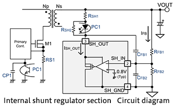
If the impedance is set too high, there is the possibility of excessive sensitivity to noise and other unstable behavior; in consideration of operation stability, RFB1 and RFB2 are selected such that IFB=10 μA or so. Given the reference voltage VREF=0.8 V (Typ) for the internal shunt regulator, VOUT is determined by the following equation.
![]()
In this design case study, VOUT is 5 V, and so RFB1 and RFB2 can be found using the following equation.
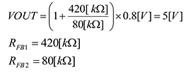
We see that because IFB=10μA for VOUT=5 V, the sum of RFB1 and RFB2 is set to 500 kΩ, and the ratio of RFB1 and RFB2 should be determined such that the voltage at the branch point (SH_IN) is 0.8 V.
Next, CFB1 and CFB2 are determined. CFB1 is a capacitor for phase compensation; a value of about 1000 pF is selected. CFB2 is a capacitor for noise elimination at the SH_IN pin; typical values are in the range of about 100 to 470 pF. In this design case study, 220 pF was used.
The output load transient response can be adjusted using the resistor RSH1 to impart a bias to the photocoupler PC1. By using a small value for RSH1, the output load transient response is made fast, and output voltage load fluctuations can be suppressed. However, there is a tradeoff between the load transient response speed and stability, and so thorough verification is necessary. In this design case study, a value of 510 Ω is used.
The resistance RSH2 sets the circuit current of the internal shunt regulator. When SH_IN=Low, the maximum value ISH_OUT_max of the SH_OUT pin current is 75 μA. Hence the relationship between the Vf minimum value Vf_min of the photocoupler PC1 and the resistance RSH2 must satisfy the following inequality.
![]()
When Vf_min of the photocoupler PC1 is set to 1.1 V, RSH2 is calculated using the following formula to be 14.7 kΩ or less.
![]()
In this design case study, a value of 12 kΩ is chosen, including a margin.
This concludes selection of the peripheral components of the shunt regulator circuit section.
AC-DC
Basic
- AC-DC Basics
- DC-DC Conversion (Regulated) System after Smoothing
- Design Procedure for AC-DC Conversion Circuits (Overview)
- Issues and considerations in AC-DC Conversion Circuit Design
- Summary
- Extra Plus Basic Knowledge
Design
-
Overview of Design Method of PWM AC-DC Flyback Converters
- Isolated Flyback Converter Basics: Flyback Converter Operation and Snubber
- Isolated Flyback Converter Basics: What are Discontinuous Mode and Continuous Mode?
- Want are Isolated Flyhback Convertors?
- Design Procedure
- Isolated Flyback Converter Basics: What is Switching AC-DC Conversion?
- Determining Power Supply Specifications
- Designing Isolated Flyback Converter Circuits
- Isolated Flyback Converter Basics: What are Characteristics of Flyback Converter?
- Designing Isolated Flyback Converter Circuits: Transformer Design (Calculating numerical values)
- Choosing an IC for Design
- Designing Isolated Flyback Converter Circuits: Transformer Design (Structural Design) – 1
- Designing Isolated Flyback Converter Circuits: Transformer Design (Structural Design) – 2
- Designing Isolated Flyback Converter Circuits: Selecting Critical Components ? MOSFET related – 1
- Designing Isolated Flyback Converter Circuits: Selecting Critical Components ? MOSFET related – 2
- Designing Isolated Flyback Converter Circuits: Selecting Critical Components ? CIN and Snubber
- Designing Isolated Flyback Converter Circuits: Selecting Critical Components ? Output Rectifier and Cout
- Designing Isolated Flyback Converter Circuits: Selecting Critical Components ? VCC of IC
- Designing Isolated Flyback Converter Circuits: Selecting Critical Components – IC Settings Etc.
- Designing Isolated Flyback Converter Circuits: Addressing EMI and Output Noise
- Example Board Layout
- Summary
-
Overview of Design Examples of AC-DC Non-isolated Buck Converters
- What are Buck Converters? – Basic Operation and Discontinuous Mode vs. Continuous Mode
- Selection of Power Supply ICs and Design Examples
- Selecting Critical Components: Input Capacitor C1 and VCC Capacitor C2
- Selecting Critical Components: Inductor L1
- Selecting Critical Components: Current Sense Resistor R1
- Selecting Critical Components: Output Capacitor C5
- Selecting Critical Components: Output Rectifying Diode D4
- EMI Countermeasures
- Board Layout and Summary
-
Introduction
- Design Procedure
- IC Used in Design
- Power Supply Specifications and Replacement Circuit
- Synchronous Rectifying Circuit Section: Selection of Synchronous Rectifying MOSFET
- Synchronous Rectification Circuit Section: Power Supply IC Selection
- Troubleshooting ①: Case When Secondary-Side MOSFET Suddenly Turns OFF
- Synchronous Rectification Circuit Section: Selection of Peripheral Circuit Components-C1, R3 at MAX_TON Pin, and VCC Pin
- Troubleshooting ②: Case When Secondary-Side MOSFET Turns On Due to Resonance Under Light Loading
- Troubleshooting ③: Case When, Due to Surge, VDS2 Rises to Above Secondary-Side MOSFET VDS Voltage
- Comparison of Efficiency of Diode Rectification and Synchronous Rectification
- Points to Note Relating to PCB Layout
- Summary
- Synchronous Rectification Circuit Section: Selection of Peripheral Circuit Components-D1, R1, R2 at DRAIN Pin
- Shunt Regulator Circuit Section: Selection of Peripheral Circuit Components
-
Introduction
- Power Supply ICs Used in Design: Optimized for SiC MOSFETs
- Design Example Circuit
- Transformer T1 Design – 1
- Transformer T1 Design – 2
- Selecting Critical Components: MOSFET Q1
- Selecting Critical Components: Input Capacitor and Balancing Resistor
- Selecting Critical Components: Switch Setting Resistors for Overload Protection Points
- Selecting Critical Components: VCC-Related Components of Power Supply ICs
- Selecting Critical Components: Components Related to Power Supply IC BO (Brownout) Pins
- Selecting Critical Components: Components Related to Snubber Circuits
- Selecting Critical Components: MOSFET Gate Drive Adjustment Circuit
- Selecting Critical Components: Output Rectifying Diode
- Selecting Critical Components: Output Capacitors, Output Setting and Control Components
- Selecting Critical Components: Current Sense Resistors and Components Related to Detection Pins
- Selecting Critical Components: Components for Dealing with EMI and Output Noise
- PCB Layout Example
- Example Circuit and Component List
- Evaluation Results: Efficiency and Switching Waveform
- Summary
Evaluation
-
What are Isolated Flyback Converters Performance Evaluation and Checkpoints?
- Overview and important features of a power supply IC used in example performance evaluation
- Design goals and circuits in performance evaluation
- Performance evaluation using an evaluation board: Measurement method and results
- Critical checkpoint: Output transient response and rising output voltage waveform
- Critical checkpoint: Measuring temperature and loss
- Critical checkpoint: Aluminum electrolytic capacitors
- Summary
- Critical checkpoint: Transformer saturation
- Critical checkpoint: MOSFET VDS and IDS, and rated voltage of output rectifier diode
- Critical checkpoint: Vcc voltage
Product Information
FAQ