AC-DC|Design
Transformer T1 Design – 1
2018.08.09
Points of this article
・The core size, primary inductance and number of turns for a transformer T1 are calculated according to the procedure described.
・Calculations can be performed according to more or less the same approach as in “Designing Isolated Flyback Converter Circuits: Transformer Design (Calculating Numerical Values)”.
From this session, we begin calculations of component values and other factors and detailed circuit design, beginning with the design of a transformer T1. Calculation procedures are described below. This is substantially the same approach as ”Designing Isolated Flyback Converter Circuits: Transformer Design (Calculating Numerical Values) “, and therefore the latter should be reviewed as well.
- ①Setting a flyback voltage VOR
- ②Calculating the primary winding inductance Lp and primary-side peak current Ippk
- ③Determining the transformer size
- ④Calculating the primary winding turns Np
- ⑤Calculating the secondary winding turns Ns
- ⑥Calculating the VCC winding turns Nd
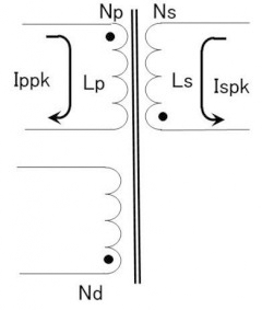
Parameters that must be derived for the transformer design are the core size, the inductance Lp, and the winding turns Np, Ns, Nd.
In addition, conditions imposed on the transformer T1 are an output of 24 V at 1 A, and VIN(DC) of from 300 V to 900 V.
The previously presented circuit diagram should be consulted as necessary.
①Setting a flyback voltage VOR
The flyback voltage VOR is equal to VO (the secondary Vout plus the VF for the secondary diode DN1) multiplied by the transformer winding ratio Np:Ns. Setting the flyback voltage VOR determines the winding ratio Np:Ns and the duty ratio. The basic equation and an example are given below. (DN1 does not appear in the circuit diagram, but the two diodes connected on the secondary side of T1 are DN1.)
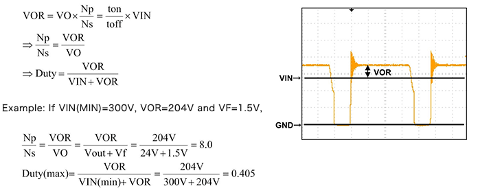
VOR should be set so that the duty is 0.5 or lower, in consideration of MOSFET losses and the like. The graph shows the MOSFET Vds waveform.
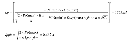
②Calculating the primary winding inductance Lp and primary-side peak current Ippk
We set the minimum oscillation frequency at minimum input voltage (VIN=300 V) to fsw=92 kHz. The other parameters are determined as follows.
- ・From Po=24V X 1A=24W, and considering overload protection and the like,?Po(max)=30 W(derating: 0.8)
- ・Transformer efficiency η=85%
- ・Resonant capacitance Cv=100pF
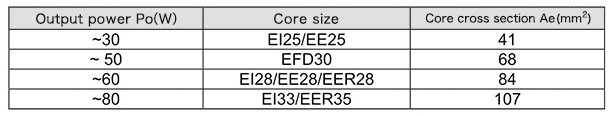
③Determining the transformer core size
Given Po(max)=30 W, a moderate margin is included to select the EFD30 core size. The following table lists core sizes that are regarded as suitable for a given output power Po. The values in the table below only represent rough approximations for output power Po. For details, transformer manufacturers should be consulted.
Thus the required core size and inductance Lp have been determined. The winding turns Np, Ns, Nd will be calculated in the next section.
Parameters Necessary for Transformer Design
| Transformer core size | EFD30 or compatible |
|---|---|
| Lp (Primary winding inductance) | 1750μH |
| Np (Primary winding turns) | (to be calculated in the next section) |
| Ns (Secondary winding turns) | (to be calculated in the next section) |
| Nd (VCC winding turns) | (to be calculated in the next section) |
AC-DC
Basic
- AC-DC Basics
- DC-DC Conversion (Regulated) System after Smoothing
- Design Procedure for AC-DC Conversion Circuits (Overview)
- Issues and considerations in AC-DC Conversion Circuit Design
- Summary
- Extra Plus Basic Knowledge
Design
-
Overview of Design Method of PWM AC-DC Flyback Converters
- Isolated Flyback Converter Basics: Flyback Converter Operation and Snubber
- Isolated Flyback Converter Basics: What are Discontinuous Mode and Continuous Mode?
- Want are Isolated Flyhback Convertors?
- Design Procedure
- Isolated Flyback Converter Basics: What is Switching AC-DC Conversion?
- Determining Power Supply Specifications
- Designing Isolated Flyback Converter Circuits
- Isolated Flyback Converter Basics: What are Characteristics of Flyback Converter?
- Designing Isolated Flyback Converter Circuits: Transformer Design (Calculating numerical values)
- Choosing an IC for Design
- Designing Isolated Flyback Converter Circuits: Transformer Design (Structural Design) – 1
- Designing Isolated Flyback Converter Circuits: Transformer Design (Structural Design) – 2
- Designing Isolated Flyback Converter Circuits: Selecting Critical Components ? MOSFET related – 1
- Designing Isolated Flyback Converter Circuits: Selecting Critical Components ? MOSFET related – 2
- Designing Isolated Flyback Converter Circuits: Selecting Critical Components ? CIN and Snubber
- Designing Isolated Flyback Converter Circuits: Selecting Critical Components ? Output Rectifier and Cout
- Designing Isolated Flyback Converter Circuits: Selecting Critical Components ? VCC of IC
- Designing Isolated Flyback Converter Circuits: Selecting Critical Components – IC Settings Etc.
- Designing Isolated Flyback Converter Circuits: Addressing EMI and Output Noise
- Example Board Layout
- Summary
-
Overview of Design Examples of AC-DC Non-isolated Buck Converters
- What are Buck Converters? – Basic Operation and Discontinuous Mode vs. Continuous Mode
- Selection of Power Supply ICs and Design Examples
- Selecting Critical Components: Input Capacitor C1 and VCC Capacitor C2
- Selecting Critical Components: Inductor L1
- Selecting Critical Components: Current Sense Resistor R1
- Selecting Critical Components: Output Capacitor C5
- Selecting Critical Components: Output Rectifying Diode D4
- EMI Countermeasures
- Board Layout and Summary
-
Introduction
- Design Procedure
- IC Used in Design
- Power Supply Specifications and Replacement Circuit
- Synchronous Rectifying Circuit Section: Selection of Synchronous Rectifying MOSFET
- Synchronous Rectification Circuit Section: Power Supply IC Selection
- Troubleshooting ①: Case When Secondary-Side MOSFET Suddenly Turns OFF
- Synchronous Rectification Circuit Section: Selection of Peripheral Circuit Components-C1, R3 at MAX_TON Pin, and VCC Pin
- Troubleshooting ②: Case When Secondary-Side MOSFET Turns On Due to Resonance Under Light Loading
- Troubleshooting ③: Case When, Due to Surge, VDS2 Rises to Above Secondary-Side MOSFET VDS Voltage
- Comparison of Efficiency of Diode Rectification and Synchronous Rectification
- Points to Note Relating to PCB Layout
- Summary
- Synchronous Rectification Circuit Section: Selection of Peripheral Circuit Components-D1, R1, R2 at DRAIN Pin
- Shunt Regulator Circuit Section: Selection of Peripheral Circuit Components
-
Introduction
- Power Supply ICs Used in Design: Optimized for SiC MOSFETs
- Design Example Circuit
- Transformer T1 Design – 1
- Transformer T1 Design – 2
- Selecting Critical Components: MOSFET Q1
- Selecting Critical Components: Input Capacitor and Balancing Resistor
- Selecting Critical Components: Switch Setting Resistors for Overload Protection Points
- Selecting Critical Components: VCC-Related Components of Power Supply ICs
- Selecting Critical Components: Components Related to Power Supply IC BO (Brownout) Pins
- Selecting Critical Components: Components Related to Snubber Circuits
- Selecting Critical Components: MOSFET Gate Drive Adjustment Circuit
- Selecting Critical Components: Output Rectifying Diode
- Selecting Critical Components: Output Capacitors, Output Setting and Control Components
- Selecting Critical Components: Current Sense Resistors and Components Related to Detection Pins
- Selecting Critical Components: Components for Dealing with EMI and Output Noise
- PCB Layout Example
- Example Circuit and Component List
- Evaluation Results: Efficiency and Switching Waveform
- Summary
Evaluation
-
What are Isolated Flyback Converters Performance Evaluation and Checkpoints?
- Overview and important features of a power supply IC used in example performance evaluation
- Design goals and circuits in performance evaluation
- Performance evaluation using an evaluation board: Measurement method and results
- Critical checkpoint: Output transient response and rising output voltage waveform
- Critical checkpoint: Measuring temperature and loss
- Critical checkpoint: Aluminum electrolytic capacitors
- Summary
- Critical checkpoint: Transformer saturation
- Critical checkpoint: MOSFET VDS and IDS, and rated voltage of output rectifier diode
- Critical checkpoint: Vcc voltage
Product Information
FAQ