AC-DC|Design
Synchronous Rectification Circuit Section: Power Supply IC Selection
2019.12.25
Points of this article
・The operation and various conditions of the existing circuit are confirmed, and the power supply IC to be used in the design is selected.
・The maximum ON time is set to prevent failure due to simultaneous ON operation of MOSFETs on the primary and secondary sides.
・The compulsion OFF time is calculated, and the relevant BM1R001xxF series model is selected.
・In the BM1R001xxF series, five models with different compulsion OFF times are provided.
As part of a procedure to convert the secondary-side diode rectification circuit of the original circuit to synchronous rectification, in the previous article we selected a MOSFET to replace the rectifying diode. Following this, operation and various conditions of the preexisting circuit are verified, and the power supply IC to be used in the design is finalized. Here, design is being performed with the object of replacing the secondary-side diode rectification circuit of an existing AC-DC converter with a synchronous rectification circuit, and so an approach is necessary in which the specifications, characteristics and operation of the existing circuit are confirmed and adjustments are made, and components are then replaced to advance toward synchronous rectification.
Synchronous Rectification Circuit Section: Power Supply IC Selection
The BM1R001xxF series that will be used in this replacement design consists of five models, the BM1R00146F through BM1R00150F. They offer a series of compulsion OFF times so as to enable synchronous rectification in power supplies with various specifications.
The compulsion OFF time prevents another turn-on operation of the secondary-side MOSFET due to the resonance waveform that occurs at the DRAIN pin of the IC under light loading. This time represents the interval, starting from when the secondary side turns off, during which turn-on is forcibly prevented; models with a compulsion OFF time of from 1.3 μs (BM1R00146F) to 4.6 μs (BM1R00150F) can be selected from the product lineup.
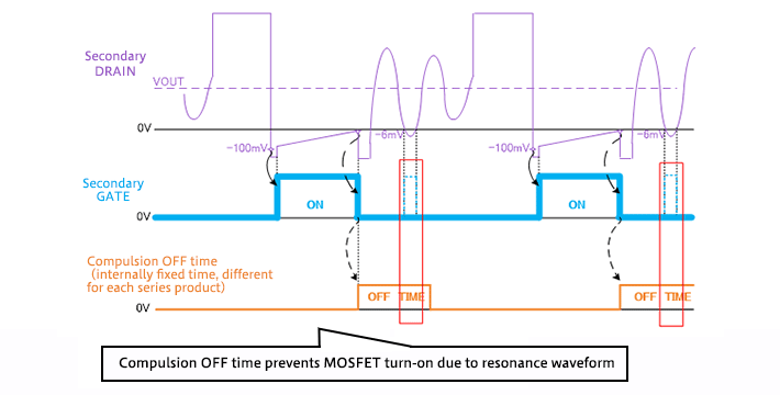
However, if this compulsion OFF time is too long, there is a time interval during which the MOSFET cannot be turned on during heavy loading, so that efficiency is worsened. Hence an appropriate time must be selected (details will be explained later).
As criteria to be used when determining the compulsion OFF time during continuous mode operation, the switching frequency of the primary-side controller and the on-times of the MOSFETs on the primary side and secondary side must be considered.
The power supply IC is selected by following the procedures (1) to (3) below.
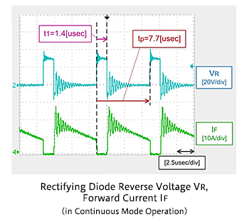
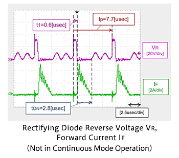
- (1)Check the waveforms of the reverse voltage VR and the forward current IF occurring in the rectifying diode DOUT prior to replacement
⇒Measure the ON-time t1 of the primary-side MOSFET M1 and one cycle tp of the primary-side controller - (2)Set the maximum ON-time tMAX_ON of the secondary-side MOSFET
⇒The tMAX_ON setting prevents failure due to simultaneous on-operation of the primary-side and secondary-side MOSFETs under heavy loads while in continuous mode - (3)IC selection
⇒Use the following equation to calculate the compulsion OFF time tOFF required, and select a model from the series
This is a method for calculating the compulsion OFF time in continuous mode operation. A method of calculation for when continuous mode operation is not performed is described later. Please refer to this method as needed.
Below, details of each procedure are explained.
(1) Check the waveforms of the reverse voltage VR and the forward current IF occurring in the rectifying diode DOUT prior to replacement
(2) Set the maximum on time tMAX_ON of the secondary-side MOSFET
The MAX_TON pin of the IC is used to set the maximum ON time tMAX_ON. When a rising voltage edge of at least VCC (= the output voltage VOUT) × 1.4 V typ is detected at the DRAIN pin, counting for the maximum ON time begins. When the maximum ON time tMAX_ON set using the resistor RTON has elapsed, the secondary-side MOSFET M2 is forcibly turned off.
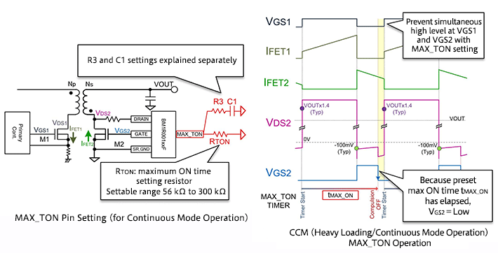
The maximum ON time tMAX_ON must always be set to be shorter than one cycle tp of the primary-side controller, as shown in the figure below. The resistor RTON can be set in the range 56 kΩ to 300 kΩ, and tMAX_ON is proportional to this resistance value. The closer the set value of tMAX_ON to 10 μs (RTON=100 kΩ), the higher the resulting precision. Please refer to the graph below.
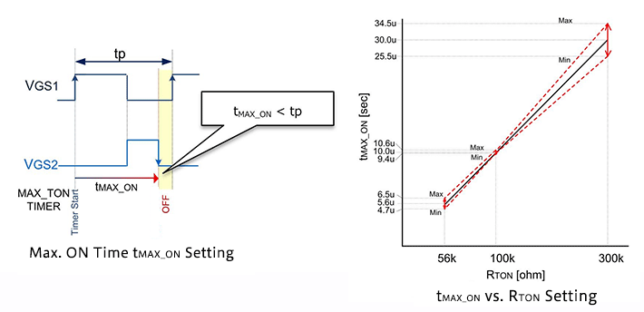
If the primary-side controller uses PWM control, a value for RTON that takes variation into consideration is determined using the following equation.
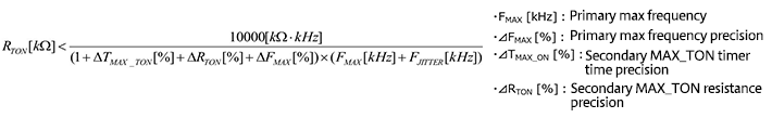
In this design example, given FMAX=130 kHz, ⊿FMAX=5%, ⊿tMAX_ON=7%, and ⊿RTON=1%, RTON is as follows.
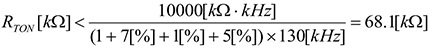
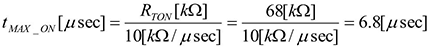
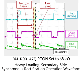
In this design example, RTON is set to 68 kΩ or lower. However, this equation is for an ideal state, and thorough checking of the operation of actual equipment is necessary. If RTON is set to 68 kΩ, then tMAX_ON can be calculated using the following equation to be 6.8 μsec.
(3) IC selection
From the primary-side MOSFET M1 ON time t1 and the primary-side controller cycle time tp measured in (1), and from the maximum ON time tMAX_ON calculated in (2), the required compulsion OFF time tOFF can be calculated using the following formula.
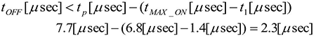
Using the above calculation result and taking variation into consideration, the model BM1R00147F, with a compulsion OFF time tOFF of 2 μs (typ.), is selected. The table below shows compulsion OFF times tOFF for the BM1R001xxF series. Variation in compulsion OFF times is ±9%. Because this formula is for an ideal state, operation in actual equipment must be checked thoroughly before setting this value.
As an example, the continuous operation (under heavy loading) secondary-side synchronous rectification operation waveform using a BM1R00147F, and with RTON = 68 kΩ, is shown. It can be seen that after tMAX_ON has elapsed VGS2 turns off, and after tOFF it is again turned on.
Here, the optimum IC for conversion of an existing power supply to synchronous rectification can be selected. This example assumes continuous mode operation, but for reference we include considerations for a case in which the existing power supply does not operate in continuous mode and a case in which the primary-side controller is provided with a jitter function.
* Method of calculating the compulsion OFF time when operation is not in continuous mode and MAX_TON pin settings
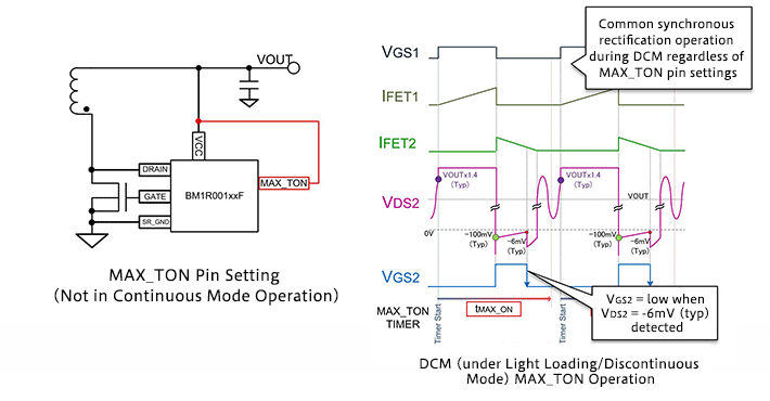
When in discontinuous mode, synchronous rectification operation is the same regardless of MAX_TON pin settings. Further, when VDS2 reaches -6 mV (typ.), VGS2 turns off.
* Case in which the primary-side controller is provided with a jitter function
The setting of RTON taking variation into account in a case in which the primary-side controller is provided with a jitter function is based on the following equation.
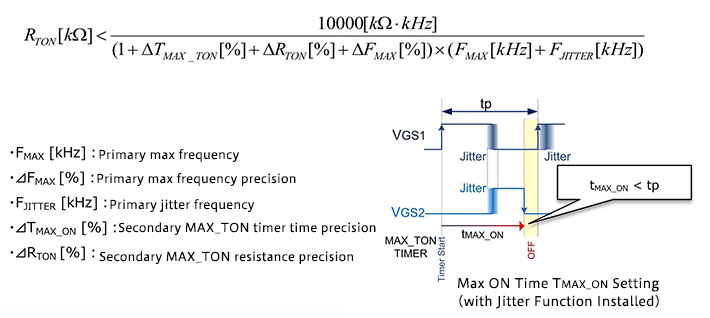
In the continuous-mode equation presented above, a primary-side jitter frequency FJITTER (kHz) is added to the denominator.
AC-DC
Basic
- AC-DC Basics
- DC-DC Conversion (Regulated) System after Smoothing
- Design Procedure for AC-DC Conversion Circuits (Overview)
- Issues and considerations in AC-DC Conversion Circuit Design
- Summary
- Extra Plus Basic Knowledge
Design
-
Overview of Design Method of PWM AC-DC Flyback Converters
- Isolated Flyback Converter Basics: Flyback Converter Operation and Snubber
- Isolated Flyback Converter Basics: What are Discontinuous Mode and Continuous Mode?
- Want are Isolated Flyhback Convertors?
- Design Procedure
- Isolated Flyback Converter Basics: What is Switching AC-DC Conversion?
- Determining Power Supply Specifications
- Designing Isolated Flyback Converter Circuits
- Isolated Flyback Converter Basics: What are Characteristics of Flyback Converter?
- Designing Isolated Flyback Converter Circuits: Transformer Design (Calculating numerical values)
- Choosing an IC for Design
- Designing Isolated Flyback Converter Circuits: Transformer Design (Structural Design) – 1
- Designing Isolated Flyback Converter Circuits: Transformer Design (Structural Design) – 2
- Designing Isolated Flyback Converter Circuits: Selecting Critical Components ? MOSFET related – 1
- Designing Isolated Flyback Converter Circuits: Selecting Critical Components ? MOSFET related – 2
- Designing Isolated Flyback Converter Circuits: Selecting Critical Components ? CIN and Snubber
- Designing Isolated Flyback Converter Circuits: Selecting Critical Components ? Output Rectifier and Cout
- Designing Isolated Flyback Converter Circuits: Selecting Critical Components ? VCC of IC
- Designing Isolated Flyback Converter Circuits: Selecting Critical Components – IC Settings Etc.
- Designing Isolated Flyback Converter Circuits: Addressing EMI and Output Noise
- Example Board Layout
- Summary
-
Overview of Design Examples of AC-DC Non-isolated Buck Converters
- What are Buck Converters? – Basic Operation and Discontinuous Mode vs. Continuous Mode
- Selection of Power Supply ICs and Design Examples
- Selecting Critical Components: Input Capacitor C1 and VCC Capacitor C2
- Selecting Critical Components: Inductor L1
- Selecting Critical Components: Current Sense Resistor R1
- Selecting Critical Components: Output Capacitor C5
- Selecting Critical Components: Output Rectifying Diode D4
- EMI Countermeasures
- Board Layout and Summary
-
Introduction
- Design Procedure
- IC Used in Design
- Power Supply Specifications and Replacement Circuit
- Synchronous Rectifying Circuit Section: Selection of Synchronous Rectifying MOSFET
- Synchronous Rectification Circuit Section: Power Supply IC Selection
- Troubleshooting ①: Case When Secondary-Side MOSFET Suddenly Turns OFF
- Synchronous Rectification Circuit Section: Selection of Peripheral Circuit Components-C1, R3 at MAX_TON Pin, and VCC Pin
- Troubleshooting ②: Case When Secondary-Side MOSFET Turns On Due to Resonance Under Light Loading
- Troubleshooting ③: Case When, Due to Surge, VDS2 Rises to Above Secondary-Side MOSFET VDS Voltage
- Comparison of Efficiency of Diode Rectification and Synchronous Rectification
- Points to Note Relating to PCB Layout
- Summary
- Synchronous Rectification Circuit Section: Selection of Peripheral Circuit Components-D1, R1, R2 at DRAIN Pin
- Shunt Regulator Circuit Section: Selection of Peripheral Circuit Components
-
Introduction
- Power Supply ICs Used in Design: Optimized for SiC MOSFETs
- Design Example Circuit
- Transformer T1 Design – 1
- Transformer T1 Design – 2
- Selecting Critical Components: MOSFET Q1
- Selecting Critical Components: Input Capacitor and Balancing Resistor
- Selecting Critical Components: Switch Setting Resistors for Overload Protection Points
- Selecting Critical Components: VCC-Related Components of Power Supply ICs
- Selecting Critical Components: Components Related to Power Supply IC BO (Brownout) Pins
- Selecting Critical Components: Components Related to Snubber Circuits
- Selecting Critical Components: MOSFET Gate Drive Adjustment Circuit
- Selecting Critical Components: Output Rectifying Diode
- Selecting Critical Components: Output Capacitors, Output Setting and Control Components
- Selecting Critical Components: Current Sense Resistors and Components Related to Detection Pins
- Selecting Critical Components: Components for Dealing with EMI and Output Noise
- PCB Layout Example
- Example Circuit and Component List
- Evaluation Results: Efficiency and Switching Waveform
- Summary
Evaluation
-
What are Isolated Flyback Converters Performance Evaluation and Checkpoints?
- Overview and important features of a power supply IC used in example performance evaluation
- Design goals and circuits in performance evaluation
- Performance evaluation using an evaluation board: Measurement method and results
- Critical checkpoint: Output transient response and rising output voltage waveform
- Critical checkpoint: Measuring temperature and loss
- Critical checkpoint: Aluminum electrolytic capacitors
- Summary
- Critical checkpoint: Transformer saturation
- Critical checkpoint: MOSFET VDS and IDS, and rated voltage of output rectifier diode
- Critical checkpoint: Vcc voltage
Product Information
FAQ