AC-DC|Design
Synchronous Rectification Circuit Section: Selection of Peripheral Circuit Components-D1, R1, R2 at DRAIN Pin
2020.01.22
Points of this article
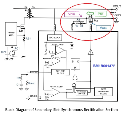
・The voltage at the DRAIN pin of the BM1R00147F controls the gate of the secondary-side MOSFET M2.
・The DRAIN pin detection level is as low as several millivolts, thus the slight surge voltage upon switching of the MOSFET M2 is erroneously detected.
・As a countermeasure, a resistor and diode are added to absorb surges at the DRAIN pin.
In the previous article, as the start of design of the synchronous rectification section, the power supply IC used in design was determined. In succession to this, the peripheral circuit components of the selected power supply IC, the BM1R00147F, are selected. In this article, D1, R1, and R2 at the DRAIN pin are selected.
Synchronous Rectification Circuit Section: Selection of Peripheral Circuit Components–D1, R1, R2 at the DRAIN Pin
Below are a circuit without a surge suppression means at the DRAIN pin, and an example of the resulting waveforms.
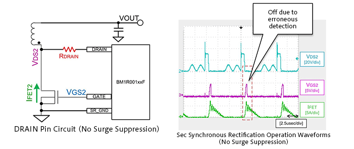
In the VDS2 waveform (blue), surges (or spikes) occur at rising edges. As a result, erroneous detection occurs, and VGS2 (purple) turns off for a shorter length of time than is normally required.
Below are shown a circuit with D1, R1, and R2 added at the DRAIN pin as a means of surge suppression, and waveform examples.
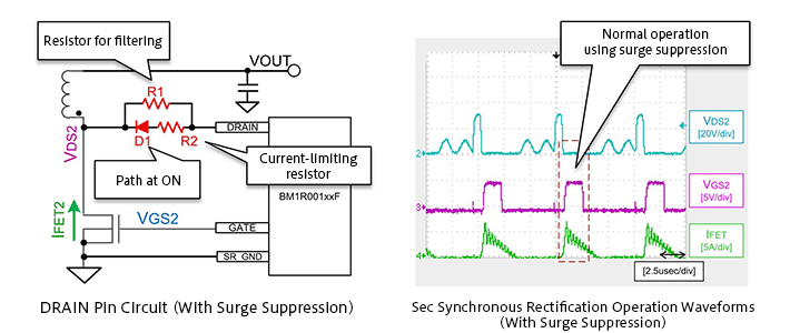
By using D1, R1, and R2 to suppress surges, VDS2 is correctly detected, and the VGS2 waveform is also normal.
With this, the reader should understand the reason for inserting D1, R1, and R2, and the effect of the insertion. Next we explain the specific component values set for each of these.
■Diode D1
The diode D1 is a current path when the MOSFET is turned on. In the circuit diagram, a simple diode symbol is shown, but a small-signal Schottky barrier diode (SBD) with a low forward voltage Vf should be selected. Because the DRAIN pin has high impedance, there is no need for D1 to have a rated voltage equal to or higher than VDS2, and a low-voltage component can be chosen. In this design example, a ROHM RB751VM-40 (VR=30 V, IO=30 mA, Vf MAX=0.37 V) is selected.
■R1
R1 is a resistor for VDS2 detection filtering. Approximately 300 Ω to 2 kΩ resistor should be inserted. The resistor should be selected while checking the VDS2 waveform and the VGS2 waveform. In this design case study, a 1 kΩ value is used. A separate more detailed explanation of setting of the R1 value is planned.
■R2
R2 is a current-limiting resistor. At the instant that the current IFET2 begins to flow in the secondary-side MOSFET M2, the MOSFET M2 is in the off state, and so IFET2 flows through the body diode of the secondary-side MOSFET M2. Therefore VDS2 = -Vf_M2 (Vf of the body diode of the MOSFET M2). The DRAIN pin of the IC is at a negative voltage, so that a current Id flows from the IC (See the figure below).
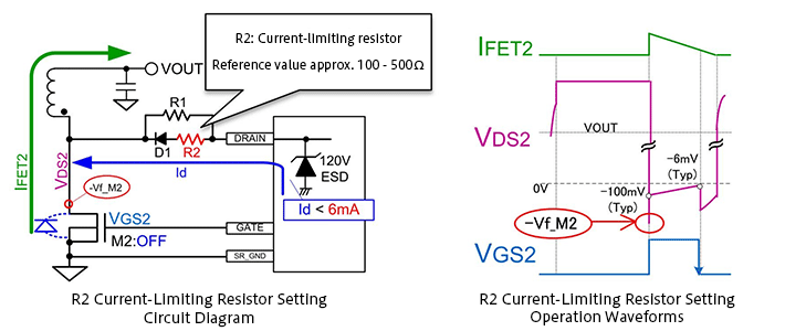
To protect the IC, R2 is selected such that the current Id flowing at this time is 6 mA or less. R2 can be calculated using the following formula.
![]()
When Vf_M2 MAX, which is the maximum value of Vf for the body diode of the MOSFET M2, is 1.2 V, Vf_D1_MIN, which is the minimum value of Vf for D1, is 0.2 V, and Vf_ESD_MIN, which is the minimum value of Vf for the ESD diode within the IC, is 0.4 V, then R2 > 100 Ω.
With a margin included, a 150 Ω resistor is selected.
AC-DC
Basic
- AC-DC Basics
- DC-DC Conversion (Regulated) System after Smoothing
- Design Procedure for AC-DC Conversion Circuits (Overview)
- Issues and considerations in AC-DC Conversion Circuit Design
- Summary
- Extra Plus Basic Knowledge
Design
-
Overview of Design Method of PWM AC-DC Flyback Converters
- Isolated Flyback Converter Basics: Flyback Converter Operation and Snubber
- Isolated Flyback Converter Basics: What are Discontinuous Mode and Continuous Mode?
- Want are Isolated Flyhback Convertors?
- Design Procedure
- Isolated Flyback Converter Basics: What is Switching AC-DC Conversion?
- Determining Power Supply Specifications
- Designing Isolated Flyback Converter Circuits
- Isolated Flyback Converter Basics: What are Characteristics of Flyback Converter?
- Designing Isolated Flyback Converter Circuits: Transformer Design (Calculating numerical values)
- Choosing an IC for Design
- Designing Isolated Flyback Converter Circuits: Transformer Design (Structural Design) – 1
- Designing Isolated Flyback Converter Circuits: Transformer Design (Structural Design) – 2
- Designing Isolated Flyback Converter Circuits: Selecting Critical Components ? MOSFET related – 1
- Designing Isolated Flyback Converter Circuits: Selecting Critical Components ? MOSFET related – 2
- Designing Isolated Flyback Converter Circuits: Selecting Critical Components ? CIN and Snubber
- Designing Isolated Flyback Converter Circuits: Selecting Critical Components ? Output Rectifier and Cout
- Designing Isolated Flyback Converter Circuits: Selecting Critical Components ? VCC of IC
- Designing Isolated Flyback Converter Circuits: Selecting Critical Components – IC Settings Etc.
- Designing Isolated Flyback Converter Circuits: Addressing EMI and Output Noise
- Example Board Layout
- Summary
-
Overview of Design Examples of AC-DC Non-isolated Buck Converters
- What are Buck Converters? – Basic Operation and Discontinuous Mode vs. Continuous Mode
- Selection of Power Supply ICs and Design Examples
- Selecting Critical Components: Input Capacitor C1 and VCC Capacitor C2
- Selecting Critical Components: Inductor L1
- Selecting Critical Components: Current Sense Resistor R1
- Selecting Critical Components: Output Capacitor C5
- Selecting Critical Components: Output Rectifying Diode D4
- EMI Countermeasures
- Board Layout and Summary
-
Introduction
- Design Procedure
- IC Used in Design
- Power Supply Specifications and Replacement Circuit
- Synchronous Rectifying Circuit Section: Selection of Synchronous Rectifying MOSFET
- Synchronous Rectification Circuit Section: Power Supply IC Selection
- Troubleshooting ①: Case When Secondary-Side MOSFET Suddenly Turns OFF
- Synchronous Rectification Circuit Section: Selection of Peripheral Circuit Components-C1, R3 at MAX_TON Pin, and VCC Pin
- Troubleshooting ②: Case When Secondary-Side MOSFET Turns On Due to Resonance Under Light Loading
- Troubleshooting ③: Case When, Due to Surge, VDS2 Rises to Above Secondary-Side MOSFET VDS Voltage
- Comparison of Efficiency of Diode Rectification and Synchronous Rectification
- Points to Note Relating to PCB Layout
- Summary
- Synchronous Rectification Circuit Section: Selection of Peripheral Circuit Components-D1, R1, R2 at DRAIN Pin
- Shunt Regulator Circuit Section: Selection of Peripheral Circuit Components
-
Introduction
- Power Supply ICs Used in Design: Optimized for SiC MOSFETs
- Design Example Circuit
- Transformer T1 Design – 1
- Transformer T1 Design – 2
- Selecting Critical Components: MOSFET Q1
- Selecting Critical Components: Input Capacitor and Balancing Resistor
- Selecting Critical Components: Switch Setting Resistors for Overload Protection Points
- Selecting Critical Components: VCC-Related Components of Power Supply ICs
- Selecting Critical Components: Components Related to Power Supply IC BO (Brownout) Pins
- Selecting Critical Components: Components Related to Snubber Circuits
- Selecting Critical Components: MOSFET Gate Drive Adjustment Circuit
- Selecting Critical Components: Output Rectifying Diode
- Selecting Critical Components: Output Capacitors, Output Setting and Control Components
- Selecting Critical Components: Current Sense Resistors and Components Related to Detection Pins
- Selecting Critical Components: Components for Dealing with EMI and Output Noise
- PCB Layout Example
- Example Circuit and Component List
- Evaluation Results: Efficiency and Switching Waveform
- Summary
Evaluation
-
What are Isolated Flyback Converters Performance Evaluation and Checkpoints?
- Overview and important features of a power supply IC used in example performance evaluation
- Design goals and circuits in performance evaluation
- Performance evaluation using an evaluation board: Measurement method and results
- Critical checkpoint: Output transient response and rising output voltage waveform
- Critical checkpoint: Measuring temperature and loss
- Critical checkpoint: Aluminum electrolytic capacitors
- Summary
- Critical checkpoint: Transformer saturation
- Critical checkpoint: MOSFET VDS and IDS, and rated voltage of output rectifier diode
- Critical checkpoint: Vcc voltage
Product Information
FAQ