SiC Power Device|Application
Behavior of the Gate-Source Voltage During Low-side Switch Turn-off
2021.03.10
Points of this article
・When the LS switch has turned off also, the same behavior as during turn-on occurs.
・Minus surges occurring on the HS may exceed the rated value, and in such cases circuit modification is necessary.
In the previous article, the behavior of the gate-source voltage at LS switch turn-on was explained. In this article, the behavior upon LS turn-off is explained in detail.
Behavior of the Gate-Source Voltage During Low-side Switch Turn-off
Below are shown schematically the current behavior in an equivalent circuit when the LS MOSFET is turned off, and waveforms in the circuit. Similarly to during turn-on, the numbers (IV), (V), and (VI) are assigned to correspond to different events. The order of change of VDS and ID is merely different from that during turn-on, and the basic operation is the same. The correspondence with the behavior during turn-on is as follows.
| Turn-off | Turn-on | |
| Event(IV) | → | Event(II) |
| Event(V) | → | Event(III) |
| Event(VI) | → | Event(I) |
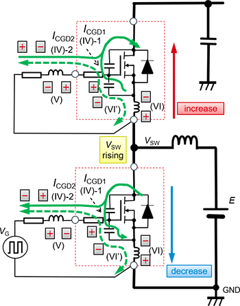
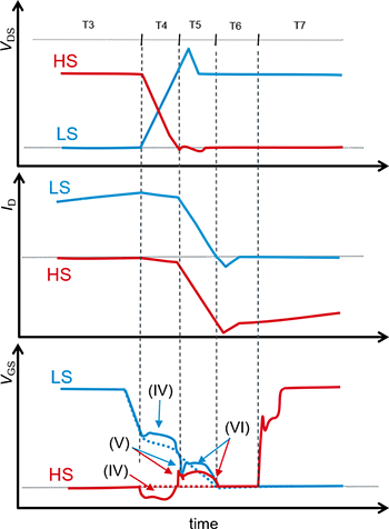
The rise in the LS VGS due to dVDS/dt and the minus surge in the HS VGS (T4 in the schematic waveform diagram) are the events (IV).
When, at the end of the period T4 in the schematic waveform diagram, ICGD1 indicated in equation (2) vanishes, the surge that then occurs is event (V). Equation (2) is the same as that presented previously. Thereafter the drain current changes (T6 in the waveform diagram), the emf caused by LSOURCE indicated in equation (1) occurs, and a current flows, indicated as event (VI) in the equivalent circuit. Equation (1) is also the same as that presented previously.
![]()
![]()
This current charges the CGS of the MOSFET with the source side as negative, so that on the HS, VGS is raised, and on the LS, VGS is pulled to the positive side, appearing as an action to impede a fall in VGS. As a result, the VGS behavior seen in the schematic waveform diagram occurs. The dotted line for VGS in the waveform diagram represents the ideal voltage waveform.
Effect of External Gate Resistors
Below we present double-pulse test results when LS is turned off in a SiC MOSFET bridge configuration. The waveform diagram (a) is for the case in which the external gate resistor RG_EXT is 0 Ω, and (b) is for when it is 10 Ω. In the diagrams, (IV), (V), and (VI) are the same as the events explained earlier.
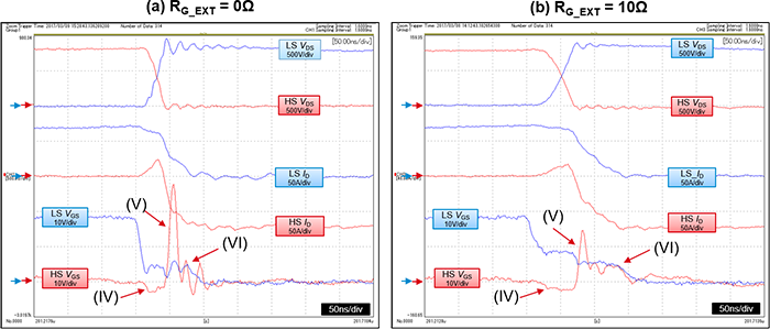
As can be seen in the diagrams, the surge in (V) appears prominently.
The influence of the event (IV) due to the change in VDS is minimal, but the minus surge due to event (IV) on the HS frequently exceeds the rated value, and in such cases the circuit must be modified. In order to reduce the HS minus surges upon turn-off, the HS gate resistor RG_EXT is decreased. However, when using a widely employed gate resistor adjustment circuit such as that explained in the previous article, the event (IV) is more pronounced for higher resistance values of RG_ON, so caution must be exercised.
Because the rise in VGS due to event (VI) occurs immediately before the end of turn-off, even when HS has entered turn-on operation, LS is turned off, and essentially no problems result.
【Download Documents】 Basics of SiC Power Devices
This handbook explains the physical properties and advantages of SiC, the differences in characteristics and usage of SiC Schottky barrier diodes and SiC MOSFETs with a comparison to Si devices, and includes a description of full SiC modules with various advantages.

SiC Power Device
Basic
- What are SiC Schottky barrier diodes? ? Introduction
- What are SiC-MOSFETs? – SiC-MOSFET Features
- What are Full-SiC Power Modules?
- Summary
- Introduction
- What is silicon carbide?
Application
-
Introduction
- SiC MOSFET Bridge Configuration
- SiC MOSFET Gate Driving Circuit and Turn-On/Turn-Off Operation
- Currents and Voltages Occurring Due to Switching in Bridge Circuits
- Behavior of the Gate-Source Voltage During Low-side Switch Turn-on
- Behavior of the Gate-Source Voltage During Low-side Switch Turn-off
- Summary
- SiC MOSFETs: Method for Determining Losses from Switching Waveforms
-
SiC MOSFETs: Snubber Circuit Designs ーIntroductionー
- Non-Discharge RCD Snubber Circuit Design
- Surges Occurring between Drain and Source
- Types and Selection of Snubber Circuits
- C Snubber Circuit Design
- RC Snubber Circuit Design
- Discharge RCD Snubber Circuit Design
- Non-Discharge RCD Snubber Circuit Design
- Differences in Surge Occurrence Depending on Package
- SiC MOSFETs: Snubber Circuit Designs ーSummaryー
- Points to Note When Measuring SiC MOSFET Gate-Source Voltages: General Measurement Methods
-
Conventional MOSFET Driving Method
- Packages Provided with Driver Source Terminals
- Differences Made by and Benefits of a Driver Source Pin
- Benefits of a Driver Source Terminal: Comparisons Using Double Pulse Tests
- Behavior of Gate-Source Voltages when in a Bridge Configuration: Behavior at Turn-on
- Behavior of Gate-Source Voltages when in a Bridge Configuration: Behavior at Turn-off
- Points to be Noted Relating to Board Wiring Layout Key Points of This Article
- Verification of Loss Reduction Using Latest-Generation SiC MOSFETs
- About Surges in Gate-Source Voltages
Product Information
- SiC Schottky Barrier Diodes
- SiC MOSFET
- SiC Power Modules
- SiC Schottky barrier diode Bare Die
- SiC MOSFET Bare Die
FAQ