SiC Power Device|Application
SiC MOSFET Bridge Configuration
2020.08.05
Points of this article
・In examining" SiC MOSFET: Behavior of Gate-Source Voltage in Bridge Configuration", the simplest synchronous boost circuit, using MOSFETs in a bridge configuration, is used as an example.
・The configuration and operation of the example circuit, and the voltage and current waveforms, should be understood.
As part of our examination of ” SiC MOSFET: Behavior of Gate-Source Voltage in Bridge Configuration”, in this article we explain the bridge configuration that is assumed and its operation.
SiC MOSFET Bridge Configuration
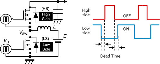
The circuit below is the simplest synchronous boost circuit that uses MOSFETs in a bridge configuration. The high-side (HS) and low-side (LS) SiC MOSFETs used in this circuit are turned on in alternation, and in order to prevent the simultaneous turn-on of both the HS and LS devices, a dead time is set, during which both the HS and the LS MOSFETs are turned off. The waveforms on the lower right indicate the timing of the gate signals (VG).
The approximate waveform shapes of the drain-source voltage (VDS) and the drain current (ID) of the HS and LS MOSFETs in this circuit are shown below. These waveforms assume a so-called hard-switching state, in which the current of the inductor L produces continuous operation.
The horizontal axis represents time; the time periods Tk (k=1 to 8) are defined as follows.
- T1: Interval in which LS is on and the MOSFET current is changing
- T2: Interval in which LS is on and the MOSFET voltage is changing
- T3: Interval in which LS is on
- T4: Interval in which LS is off and the MOSFET voltage is changing
- T5: Interval in which LS is off and the MOSFET current is changing
- T4 to T6: Dead time intervals preceding turn-on of HS
- T7: Interval in which HS is turned on (synchronous rectification interval)
- T8: Dead time interval from turn-off of HS to turn-on of LS
The discussion beginning in the next article will assume the above, and so the operation of this bridge circuit, and the voltage and current waveforms, should be thoroughly grasped.
【Download Documents】 Basics of SiC Power Devices
This handbook explains the physical properties and advantages of SiC, the differences in characteristics and usage of SiC Schottky barrier diodes and SiC MOSFETs with a comparison to Si devices, and includes a description of full SiC modules with various advantages.

SiC Power Device
Basic
- What are SiC Schottky barrier diodes? ? Introduction
- What are SiC-MOSFETs? – SiC-MOSFET Features
- What are Full-SiC Power Modules?
- Summary
- Introduction
- What is silicon carbide?
Application
-
Introduction
- SiC MOSFET Bridge Configuration
- SiC MOSFET Gate Driving Circuit and Turn-On/Turn-Off Operation
- Currents and Voltages Occurring Due to Switching in Bridge Circuits
- Behavior of the Gate-Source Voltage During Low-side Switch Turn-on
- Behavior of the Gate-Source Voltage During Low-side Switch Turn-off
- Summary
- SiC MOSFETs: Method for Determining Losses from Switching Waveforms
-
SiC MOSFETs: Snubber Circuit Designs ーIntroductionー
- Non-Discharge RCD Snubber Circuit Design
- Surges Occurring between Drain and Source
- Types and Selection of Snubber Circuits
- C Snubber Circuit Design
- RC Snubber Circuit Design
- Discharge RCD Snubber Circuit Design
- Non-Discharge RCD Snubber Circuit Design
- Differences in Surge Occurrence Depending on Package
- SiC MOSFETs: Snubber Circuit Designs ーSummaryー
- Points to Note When Measuring SiC MOSFET Gate-Source Voltages: General Measurement Methods
-
Conventional MOSFET Driving Method
- Packages Provided with Driver Source Terminals
- Differences Made by and Benefits of a Driver Source Pin
- Benefits of a Driver Source Terminal: Comparisons Using Double Pulse Tests
- Behavior of Gate-Source Voltages when in a Bridge Configuration: Behavior at Turn-on
- Behavior of Gate-Source Voltages when in a Bridge Configuration: Behavior at Turn-off
- Points to be Noted Relating to Board Wiring Layout Key Points of This Article
- Verification of Loss Reduction Using Latest-Generation SiC MOSFETs
- About Surges in Gate-Source Voltages
Product Information
- SiC Schottky Barrier Diodes
- SiC MOSFET
- SiC Power Modules
- SiC Schottky barrier diode Bare Die
- SiC MOSFET Bare Die
FAQ