SiC Power Device|Application
Place of Installation of Probe Heads
2024.08.07
Points of this article
・In addition to the measurement location, the position of installation of probe heads is also important.
・If probe heads are carelessly installed in a space where there are rapid changes in magnetic flux, the effect of the changing magnetic flux may be superposed on the measured waveform.
Points to Note When Measuring SiC MOSFET Gate-Source Voltages: Place of Installation of Probe Heads
In addition to the measurement points explained previously, there is one other matter that must be born in mind: the place at which the heads of a voltage probe are installed.
In general, in environments where power switching devices are used, large currents ranging from tens to hundreds of Amps are switched rapidly, and so the magnetic flux changes dΦ/dt that occurs due to the current changes di/dt are also extremely large. Moreover, voltage changes dv/dt are also very large, with extremely high voltages occurring, and consequently the changes in the current that flows during voltage changes are not at all small.
If a voltage probe is installed carelessly in a space in which such rapid flux changes occur, the probe heads may be affected by the flux changes, with the effect of the flux changes superposed on the measured waveform. Below, the switching waveforms when using four different installation methods are compared.
(a) Probe heads inside the main circuit loop
(b) Probe heads on the outside and very close to the main current loop
(c) Outside the main circuit loop, connected with 12cm of twisted wire
(d) Outside the main circuit loop, connected with 12cm of twisted wire + 100Ω
Fig. 11(a) through (d) show the different probe head installation places, and arrows indicate the current paths of the main circuit loop in each case.
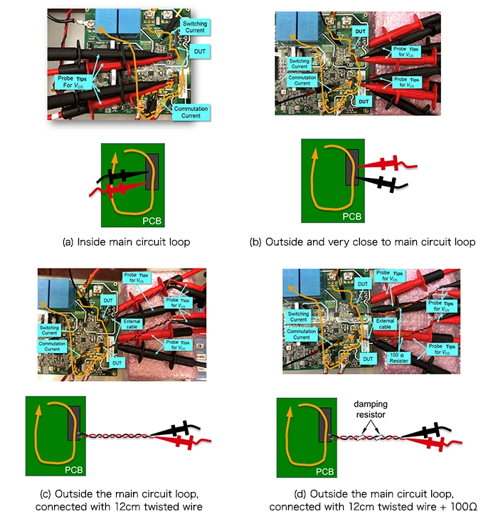
Fig. 11. Probe head installation places and main circuit loop current paths
In (a), the probe heads are placed on the inside of the main circuit loop where dΦ/dt is greatest, whereas in (b) the probe heads are installed on the outside of the main circuit loop, but because they are very close by, dΦ/dt is comparatively high. In (c) and (d), the probe heads are moved away from the main circuit loop using an extension cable, at locations where the effect of dΦ/dt is eliminated insofar as possible. However, a difference is that 100 Ω damping resistors are inserted in the case of (d).
Fig. 12 shows gate-source voltage waveforms observed for each of the above four installation methods.
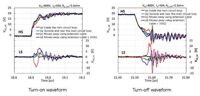
Fig. 12. Differences in measured waveforms for different probe head installation locations
Focusing on the LS, in the case of (a) with the largest magnetic flux changes, surges occur with the same timing as switching operation, and we see that the effect of radiated emission is considerable. In the case of (c), the inductance of the extension cable causes greater fluctuations than for (b). The smallest fluctuations resulted for (d), in which a 100 Ω damping resistors were inserted into the extension cable to suppress ringing.
In these measurements, switching is on the HS, and so the LS gate voltage is always in the off state (0 V). Consequently there is absolutely no driving current flowing to the gate terminal, and it is expected that operation is easily affected by flux changes. On the other hand, on the HS a charging current for driving is flowing to the SiC MOSFET gate terminal during switching operation, so that the operation is not easily affected, and possibly for this reason, the waveform is not as disrupted as on the LS side.
SiC Power Device
Basic
- What are SiC Schottky barrier diodes? ? Introduction
- What are SiC-MOSFETs? – SiC-MOSFET Features
- What are Full-SiC Power Modules?
- Summary
- Introduction
- What is silicon carbide?
Application
-
Introduction
- SiC MOSFET Bridge Configuration
- SiC MOSFET Gate Driving Circuit and Turn-On/Turn-Off Operation
- Currents and Voltages Occurring Due to Switching in Bridge Circuits
- Behavior of the Gate-Source Voltage During Low-side Switch Turn-on
- Behavior of the Gate-Source Voltage During Low-side Switch Turn-off
- Summary
- SiC MOSFETs: Method for Determining Losses from Switching Waveforms
-
SiC MOSFETs: Snubber Circuit Designs ーIntroductionー
- Non-Discharge RCD Snubber Circuit Design
- Surges Occurring between Drain and Source
- Types and Selection of Snubber Circuits
- C Snubber Circuit Design
- RC Snubber Circuit Design
- Discharge RCD Snubber Circuit Design
- Non-Discharge RCD Snubber Circuit Design
- Differences in Surge Occurrence Depending on Package
- SiC MOSFETs: Snubber Circuit Designs ーSummaryー
- Points to Note When Measuring SiC MOSFET Gate-Source Voltages: General Measurement Methods
-
Conventional MOSFET Driving Method
- Packages Provided with Driver Source Terminals
- Differences Made by and Benefits of a Driver Source Pin
- Benefits of a Driver Source Terminal: Comparisons Using Double Pulse Tests
- Behavior of Gate-Source Voltages when in a Bridge Configuration: Behavior at Turn-on
- Behavior of Gate-Source Voltages when in a Bridge Configuration: Behavior at Turn-off
- Points to be Noted Relating to Board Wiring Layout Key Points of This Article
- Verification of Loss Reduction Using Latest-Generation SiC MOSFETs
- About Surges in Gate-Source Voltages
Product Information
- SiC Schottky Barrier Diodes
- SiC MOSFET
- SiC Power Modules
- SiC Schottky barrier diode Bare Die
- SiC MOSFET Bare Die
FAQ