SiC Power Device|Basic
Tips for Practical Use: Snubber Capacitors
2018.10.11
Points of this article
・In order to exploit high-speed switching performance, parasitic inductances in electric wiring must be suppressed insofar as possible.
・Capacitors are connected near power terminals to reduce wiring inductance.
In this article, we explain snubber capacitors used with full-SiC power modules. Snubber capacitors must be added to circuits that rapidly switch large currents.
What is a Snubber Capacitor?
A snubber capacitor is a capacitor that is connected to a large-current switching node for the purpose of reducing the parasitic inductance of electric wiring. Parasitic inductance causes large surges at switch-off (when the current is blocked), and should such surges exceed component ratings, there are concerns of consequent failure in the worst case.
In order to effectively reduce wiring inductance, capacitors must be connected near the lines indicated by the red ovals in the circuit diagram.

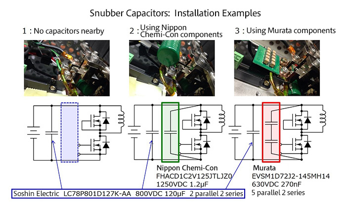
Examples of snubber capacitors
A snubber capacitor must have electrical ratings to cope with the conditions of the connection location, and moreover must be evaluated before use, including differences in characteristics arising from the capacitor structure and materials. As examples, the following capacitors were evaluated.

Examples of Snubber Capacitor Installation
In these examples, small-value capacitors are installed close to SiC MOSFET terminals, adhering to the basic principle of placing large capacitances between lines.
Effect of Snubber Capacitors
The surge waveforms occurring between drain and source when the SiC MOSFET is turned off and current is cut off are shown for the above three conditions. When a capacitor is added near the terminals of the SiC MOSFET, there is a surge suppression effect, and the effect differs depending on the type of capacitor.

Next, suppression effect waveforms are compared for the example of a ceramic capacitor (in red above), with the conditions changed.

The ringing t1 at a frequency of about 23 MHz immediately after turn-off attenuates more rapidly for fewer capacitor groups in parallel (blue A). This is thought to be because the capacitor ESR is inversely proportional to the number of parallel groups, that is, the smaller the number of parallel capacitor groups, the greater the ESR.
When the capacitance of a ceramic capacitor is small, ringing t2 at a frequency of about 2 MHz occurs (green B, blue A). This is attributed to charge that has accumulated in pathways of large loops, with large inductance.
As a result, in the case of ceramic capacitors, we can say that the surge suppression effect is greater for a smaller number of parallel groups and for larger total capacitance.
Finally, the effect of large-value capacitors is checked. Below, surges are compared when large-capacitance capacitors are and are not present, in a state in which five groups of two series-connected ceramic capacitors are connected in parallel.

As indicated by the red waveform for the case in which a large-capacitance capacitor is present, we see that a large-value capacitor is effective in suppressing long-period ringing.
In these examples, by connecting a large-value capacitor and ceramic capacitors close to the terminals of the SiC MOSFET as snubbers, a considerable suppression effect is obtained. However, the position of capacitor installation, the combination of parallel and series connections of capacitors, and slight differences affect the surge waveform, and so it is necessary to verify the suppression effect in actual equipment.
【Download Documents】 Basics of SiC Power Devices
This handbook explains the physical properties and advantages of SiC, the differences in characteristics and usage of SiC Schottky barrier diodes and SiC MOSFETs with a comparison to Si devices, and includes a description of full SiC modules with various advantages.

SiC Power Device
Basic
- What are SiC Schottky barrier diodes? ? Introduction
- What are SiC-MOSFETs? – SiC-MOSFET Features
- What are Full-SiC Power Modules?
- Summary
- Introduction
- What is silicon carbide?
Application
-
Introduction
- SiC MOSFET Bridge Configuration
- SiC MOSFET Gate Driving Circuit and Turn-On/Turn-Off Operation
- Currents and Voltages Occurring Due to Switching in Bridge Circuits
- Behavior of the Gate-Source Voltage During Low-side Switch Turn-on
- Behavior of the Gate-Source Voltage During Low-side Switch Turn-off
- Summary
- SiC MOSFETs: Method for Determining Losses from Switching Waveforms
-
SiC MOSFETs: Snubber Circuit Designs ーIntroductionー
- Non-Discharge RCD Snubber Circuit Design
- Surges Occurring between Drain and Source
- Types and Selection of Snubber Circuits
- C Snubber Circuit Design
- RC Snubber Circuit Design
- Discharge RCD Snubber Circuit Design
- Non-Discharge RCD Snubber Circuit Design
- Differences in Surge Occurrence Depending on Package
- SiC MOSFETs: Snubber Circuit Designs ーSummaryー
- Points to Note When Measuring SiC MOSFET Gate-Source Voltages: General Measurement Methods
-
Conventional MOSFET Driving Method
- Packages Provided with Driver Source Terminals
- Differences Made by and Benefits of a Driver Source Pin
- Benefits of a Driver Source Terminal: Comparisons Using Double Pulse Tests
- Behavior of Gate-Source Voltages when in a Bridge Configuration: Behavior at Turn-on
- Behavior of Gate-Source Voltages when in a Bridge Configuration: Behavior at Turn-off
- Points to be Noted Relating to Board Wiring Layout Key Points of This Article
- Verification of Loss Reduction Using Latest-Generation SiC MOSFETs
- About Surges in Gate-Source Voltages
Product Information
- SiC Schottky Barrier Diodes
- SiC MOSFET
- SiC Power Modules
- SiC Schottky barrier diode Bare Die
- SiC MOSFET Bare Die
FAQ