SiC Power Device|Application
Currents and Voltages Occurring Due to Switching in Bridge Circuits
2020.11.11
Points of this article
・Due to changes in the VDS and ID of MOSFETs in switching operation in gate driving circuits, parasitic capacitances and inductances cause currents and voltages to appear in the circuits.
・Because dVDS/dt and dID/dt assume both positive and negative values, the polarities of the resulting currents and voltages are different during turn-on and turn-off.
In the previous article, the turn-on and turn-off operation of the gate driving circuit in a SiC MOSFET bridge configuration was explained. In this article, we explain the currents and voltages that occur due to changes in the MOSFET VDS and ID during this series of switching operations.
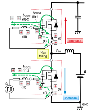
The circuit diagram below is an example of a synchronous boost circuit with a bridge configuration, when the LS switch is turned on. In the circuit diagram, the parasitic capacitances, inductances, and resistances of the SiC MOSFETs are also represented, and the gate currents (green lines) that flow in places due to changes in the VDS and ID of the HS and LS SiC MOSFETs are also shown.
Voltages Occurring Due to dID/dt, Rate of Change of ID
Because of the change in ID, the voltages indicated in equation (1) below occur.
![]()
These voltages occur because the current ID flows in the parasitic inductances that are present at the sources of the SiC MOSFETs; they occur at the sections labeled (I) in the circuit diagram. Because of these voltages, currents (I’) flow.
Currents Occurring Due to dVDS/dt, the Rate of Change of VDS
Taking the HS as an example, when the SiC MOSFET turns off and VDS changes, a current ICGD flows in the parasitic capacitance CGD between the gate and the drain. As indicated in the circuit diagram, this current splits into a current ICGD1: (II)-1 flowing on the side of the gate-source parasitic capacitance CGS, and a current ICGD2: (II)-2 flowing on the side of the gate circuit. Because prior to the beginning of the change in VDS the impedance on the gate circuit side is high, nearly all of ICGD flows to the CGS side, and at this time ICDG1 is as indicated in equation (2).
![]()
From the equation, it is seen that when CGD is large or when CGD/CGS is small, ICGD1 becomes large.
Because dVDS/dt and dID/dt take on both positive and negative values, the polarities of the currents and voltages that occur as a result are different during turn-on and during turn-off. This will be discussed in detail in the next article.
【Download Documents】 Basics of SiC Power Devices
This handbook explains the physical properties and advantages of SiC, the differences in characteristics and usage of SiC Schottky barrier diodes and SiC MOSFETs with a comparison to Si devices, and includes a description of full SiC modules with various advantages.

SiC Power Device
Basic
- What are SiC Schottky barrier diodes? ? Introduction
- What are SiC-MOSFETs? – SiC-MOSFET Features
- What are Full-SiC Power Modules?
- Summary
- Introduction
- What is silicon carbide?
Application
-
Introduction
- SiC MOSFET Bridge Configuration
- SiC MOSFET Gate Driving Circuit and Turn-On/Turn-Off Operation
- Currents and Voltages Occurring Due to Switching in Bridge Circuits
- Behavior of the Gate-Source Voltage During Low-side Switch Turn-on
- Behavior of the Gate-Source Voltage During Low-side Switch Turn-off
- Summary
- SiC MOSFETs: Method for Determining Losses from Switching Waveforms
-
SiC MOSFETs: Snubber Circuit Designs ーIntroductionー
- Non-Discharge RCD Snubber Circuit Design
- Surges Occurring between Drain and Source
- Types and Selection of Snubber Circuits
- C Snubber Circuit Design
- RC Snubber Circuit Design
- Discharge RCD Snubber Circuit Design
- Non-Discharge RCD Snubber Circuit Design
- Differences in Surge Occurrence Depending on Package
- SiC MOSFETs: Snubber Circuit Designs ーSummaryー
- Points to Note When Measuring SiC MOSFET Gate-Source Voltages: General Measurement Methods
-
Conventional MOSFET Driving Method
- Packages Provided with Driver Source Terminals
- Differences Made by and Benefits of a Driver Source Pin
- Benefits of a Driver Source Terminal: Comparisons Using Double Pulse Tests
- Behavior of Gate-Source Voltages when in a Bridge Configuration: Behavior at Turn-on
- Behavior of Gate-Source Voltages when in a Bridge Configuration: Behavior at Turn-off
- Points to be Noted Relating to Board Wiring Layout Key Points of This Article
- Verification of Loss Reduction Using Latest-Generation SiC MOSFETs
- About Surges in Gate-Source Voltages
Product Information
- SiC Schottky Barrier Diodes
- SiC MOSFET
- SiC Power Modules
- SiC Schottky barrier diode Bare Die
- SiC MOSFET Bare Die
FAQ