Electrical Circuit Design|Basic
Impedance Matching: Why It Matters for Power Transfer and Signal Reflections
2026.03.11
table of contents
Impedance matching is a basic yet powerful technique for efficiently transferring signals and power between circuits. When impedances do not match, the effects are easy to see in practice: antennas fail to radiate RF power effectively, high-speed digital signals become distorted, and audio systems suffer from degraded sound. Impedance matching is therefore an essential requirement in RF circuits, high-speed digital systems, and audio equipment.
This article explains what impedance matching is, why it is needed from the viewpoints of power transfer and signal reflections, and how it is used in practical applications such as RF, digital, and audio circuits. Finally, it outlines basic matching methods using resistors, LC networks, and transformers.
Definition and Overview of Impedance Matching
Impedance matching focuses on “making impedances consistent” between circuits that are connected. By adjusting the relationship between the source and load impedances, you can improve power transfer and suppress signal reflections.
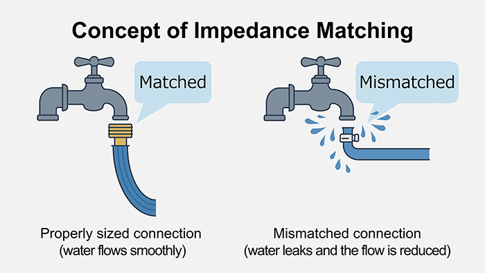
A mechanical analogy is a water faucet and a hose. If the hose diameter is much smaller than the faucet outlet, water flow is restricted, and pressure rises at the junction. If the hose is too large, the water flow becomes unstable and splashes. In the same way, in electrical circuits, the “size” of the source and the load, expressed as impedance, needs to be matched to transfer power and signals efficiently.
What Is Impedance Matching
Impedance matching is the technique of adjusting the impedance of the signal source and the load so that power and a signal can be transferred efficiently between them. When impedances are different, part of the incident wave is reflected at the connection point and returns toward the source. As a result, only a portion of the power reaches the load, and the load waveforms become distorted.
For example, if you connect a 50 Ω coaxial cable directly to a 75 Ω device, the 50 Ω line “expects” to see 50 Ω at its end, but instead it sees 75 Ω. The mismatch causes part of the signal to reflect toward the source, reducing usable power and degrading signal quality.
Why Impedance Matching Is Needed (Power Transfer and Signal Reflection)
The reasons impedance matching is essential can be summarized into two main viewpoints. The first is power transfer efficiency. If impedances are poorly matched, most of the power the source can supply is lost within the source itself. The second is signal reflection. Reflections at impedance discontinuities cause waveform distortion and can lead directly to bit errors in digital systems or to degraded sound quality in audio systems.
The sections below first discuss power transfer efficiency, and then describe how impedance mismatch generates reflections.
Power Transfer Efficiency and Maximum Power Conditions
Two Definitions of Efficiency
When power is transferred from a source to a load, there are two commonly used but easily confused efficiency definitions.
The first is the power delivery ratio η. This compares the power actually delivered to the load to the available power that a Thevenin-equivalent source can deliver under optimum loading conditions. If the source impedance and load impedance can both be treated as pure resistances Rs and RL, the power delivery ratio is
\(η=\displaystyle\frac{4R_s R_L}{(R_s+R_L)^2}\)
Here, Pavailable is the maximum power that can be obtained from the source when the load is optimally chosen. From this expression, it is clear that when
\(R_s=R_L,\ η=1\)
In other words, when the load resistance equals the source resistance, the power delivered to the load reaches 100% of the available power. In this sense, RS = RL is the maximum power transfer condition with respect to the available power.
The second definition is the actual efficiency η′. This compares the power consumed in the load to the total power that the source is actually delivering under that load condition. For the same pure resistances RS and RL, the actual efficiency is
\(η^{\ ‘}=\displaystyle\frac{R_L}{R_s+R_L}\)
Under the same condition, RS = RL, this gives
\(η^{\ ‘}=\displaystyle\frac{1}{2}\)
That is, the load consumes 50% of the supplied power, and the remaining 50% is lost inside the source resistance. The critical point is that η (defined with respect to available power) and η′ (described with respect to supplied power) are distinct indicators, and their numerical values differ. They must not be mixed up.
Maximum Power Transfer in Complex Impedance Systems
In real RF circuits or systems that include transmission lines, the source impedance ZS and load impedance ZL are generally complex impedances rather than simple resistances. Both the resistive and reactive parts must be considered.
In such systems, the condition that maximizes the power delivered to the load is well-known: the load impedance must be the complex conjugate of the source impedance. In other words,
\(Z_L=Z_s^*\)
This is called the conjugate matching condition. Under this condition, the load extracts the maximum possible power from the source. However, the expressions for η and η′ then involve the real parts and magnitudes of ZS and ZL, and become more complicated than the simple formulas for RS and RL. You cannot simply replace RS and RL in the real-valued expressions above with complex ZS and ZL. The simple formulas are valid only when both impedances are purely resistive.
Matching to a Transmission Line Characteristic Impedance
When a transmission line is inserted between the source and the load, matching must also be considered with respect to the line’s characteristic impedance Z0.
On the load side, the basic condition is
\(Z_L=Z_0\)
This eliminates reflections at the load end. On the source side, if the source impedance is also set equal to Z0, then any reflections generated by residual mismatches along the line propagate back to the source end and are absorbed there without being re-reflected toward the load. As a result, the entire system, including the transmission line, is matched with respect to Z0, and both power transfer efficiency and waveform integrity are improved.
In RF and high-speed digital systems, it is common to design the entire signal path so that “everything is matched to Z0” in this sense.
Signal Reflection Mechanisms
Reflection Coefficient at an Impedance Discontinuity
At any point where the impedance seen by a traveling wave changes abruptly, part of the wave is reflected. The ratio of the reflected wave amplitude to the incident wave amplitude is described by the reflection coefficient Γ.
For a transmission line of characteristic impedance terminated by a load impedance ZL, the reflection coefficient at the load is
\(Γ=\displaystyle\frac{Z_L-Z_0}{Z_L+Z_0}\)
When the line is perfectly matched (ZL = Z0), the numerator becomes zero, so ∣Γ∣=0 and no reflection occurs. In contrast, in the extreme cases of open circuit (ZL = ∞) or short circuit (ZL = 0), the magnitude becomes ∣Γ∣=1, meaning that the incident wave is totally reflected.
Because reflections return toward the source, they can cause power to be wasted in the source circuit, leading to local overvoltage or overcurrent conditions. In wireless transmitters, this may increase power amplifier heating and even activate protection circuits. In audio and other analog applications, reflections can cause amplitude ripples over frequency. However, audible effects are usually influenced by many different factors, such as cable structure, contact quality, and measurement conditions.
In high-speed digital circuits, reflections can cause additional transitions, slightly increasing dynamic current. Still, the dominant source of IC power dissipation remains switching loss, often approximated by a term proportional to load capacitance, the supply voltage squared, the clock frequency, and signal activity. Reflection losses are usually a secondary contribution compared to the central switching component.
Troubles Caused by Impedance Mismatch
When impedances are mismatched, circuit performance degrades in several ways. Power that should reach the load is wasted, signal waveforms are distorted, and in severe cases, devices may be damaged. This section introduces the main problems from the viewpoints of power loss and reflections.
Power Loss and Reduced Transmission Efficiency
If the reflection coefficient at the load is Γ, then the reflected power and transmitted power can be expressed simply in terms of ∣Γ∣.
The fraction of incident power that is reflected is
\(P_{reflected}=|Γ|^2 P_{incident}\)
The fraction of power that actually reaches the load is
\(P_{transmitted}=(1-|Γ|^2 ) P_{incident} \)
As a concrete example, consider a 50 Ω system with a 25 Ω load. In this case,
\(Γ=\displaystyle\frac{25-50}{25+50}=\displaystyle\frac{-25}{75}=-\displaystyle\frac{1}{3}\)
\(|Γ|^2=\displaystyle\frac{1}{9}≈0.11\)
About 11% of the incident power is reflected, leaving only about 89% to reach the load. In applications with large transmit power, even this level of mismatch can be problematic.
Impact in Practical RF Circuits
In a mobile phone transmitter, an antenna mismatch causes several issues. Some of the transmitted power is reflected and dissipated as heat in the power amplifier rather than radiated. Radiated power is reduced, communication range is shortened, and increased internal losses raise device temperature. If the mismatch becomes severe, protection circuits in the RF front end may limit output to prevent damage.
A common way to express a mismatch in RF systems is VSWR (Voltage Standing Wave Ratio). For example, VSWR = 3:1 corresponds to ∣Γ∣=0.5. In this case, 25% of the incident power is reflected. This is one reason antenna matching is considered an important design task.
Signal Reflections and VSWR (Voltage Standing Wave Ratio)
The reflected wave generated at the load travels back along the line and overlaps with the incident wave. The result is a pattern of standing waves, where the voltage amplitude changes periodically along the length of the line. VSWR indicates the degree of standing-wave formation.
VSWR is defined by the ratio of maximum to minimum voltage along the line:
\(VSWR=\displaystyle\frac{1+|Γ|}{1-|Γ|}\)
Conversely, if VSWR is known, the magnitude of the reflection coefficient can be recovered as
\(|Γ|=\displaystyle\frac{VSWR-1}{VSWR+1}\)
In an ideal match, VSWR = 1.0 and ∣Γ∣=0. For VSWR = 1.5, ∣Γ∣= 0.2, and only about 4% of the power is reflected. For VSWR = 2.0, ∣Γ∣≈0.33, and about 11% of the power is reflected. VSWR = 3.0 corresponds to ∣Γ∣= 0.5, 25% reflected power, which is usually considered poor.
In high-speed digital circuits, reflections distort signal edges, degrade eye diagrams, and cause setup and hold time violations. Even if the average power loss is not significant, the timing uncertainty and waveform distortion caused by reflections can severely degrade system reliability.
Representative Applications of Impedance Matching
Impedance matching is not a specialized technique reserved for RF specialists. It is used in many familiar devices: smartphones, computers, and audio systems. This section describes typical applications in RF circuits and antennas, high-speed digital lines, and audio equipment.
RF Circuits and Antennas (50 Ω Systems)
RF circuits process radio-frequency signals using amplifiers, filters, mixers, and other functional blocks. In many RF systems, 50 Ω is adopted as the standard impedance. This value represents a compromise between minimum loss and maximum power handling in coaxial cables.
Theoretically, coaxial cable loss is minimized around 77 Ω, while maximum power handling is achieved around 30 Ω. By choosing 50 Ω, both loss and power handling are reasonably balanced. For this reason, RF amplifiers, antennas, and cables are commonly designed with 50 Ω input and output impedance. When all blocks are unified to a typical characteristic impedance, system-level matching becomes easier, and efficiency improves.
As a design example, consider a 900-MHz-band RF amplifier. The input impedance must match so that the 50 Ω signal from the antenna is correctly transformed to the amplifier’s input impedance. The output must also be matched to 50 Ω to deliver power efficiently to the following stage or antenna without oscillation. In practice, the device’s S-parameters (S11, S21, S12, S22) are measured, and matching networks are designed on a Smith chart using combinations of capacitors, inductors, and microstrip stubs.
For antennas, a theoretical half-wave dipole has a radiation resistance of about 73 Ω. Still, by adjusting the feed-point structure and adding matching networks, the input impedance is usually brought close to 50 Ω. In mobile phones and other compact devices, chip antennas are combined with small LC matching circuits to achieve 50 Ω matching over the desired frequency band.
High-Speed Digital Signals (Termination Resistors)
In modern digital equipment, multi-gigabit-per-second signals travel along PCB traces. At these speeds, the traces behave like transmission lines, and their characteristic impedance and terminations must be carefully designed. Even modest reflections can cause overshoot, undershoot, and ringing, leading to data errors.
To control reflections, signal lines are given a target impedance (e.g., 40 Ω or 50 Ω), and termination resistors are used to match it. Common termination styles include parallel termination, Thevenin termination, and AC termination.
In parallel termination, a resistor equal to the line impedance is connected at the receiver end. This is simple and reliable, but because a DC flows continuously through the termination, static power consumption can be significant.
In the Thevenin termination, two resistors form a voltage divider between the supply and ground, and the midpoint is connected to the line. Properly selecting the resistor values allows termination with reduced DC.
In AC termination, a series combination of a resistor and a capacitor is connected to the line. The capacitor blocks DC, reducing power consumption, but the termination becomes frequency-dependent.
As an example, DDR4-3200 (1600 MHz clock) specifies approximately 40 Ω ± 10% for data lines and 40 Ω ± 5% for clocks. On-die terminations in the DRAM and the controller are adjustable (for example, 60 Ω, 120 Ω, 240 Ω), and drive strengths are calibrated so that the effective impedance seen on the line stays close to the target. Reflections are thereby suppressed during the round-trip between the CPU and memory devices.
Audio Equipment (Low Output, High Input)
In audio systems, the basic principle is often described as “low output, high input”. Rather than trying to achieve maximum power transfer with equal impedances, designers deliberately set the source impedance low and the load impedance high. This minimizes signal loss and reduces the influence of cable and load variations.
If the source has output impedance Ro and the load has input impedance Ri, the voltage division ratio between the input and the output is
\(\displaystyle\frac{V_{out}}{V_{in}} = \displaystyle\frac{R_i}{R_o+R_i}\)
When Ri » Ro, the ratio becomes very close to 1, so the signal amplitude is hardly reduced. This also means that connecting multiple loads in parallel has only a negligible effect on the overall signal level.
Typical impedance values in audio equipment are as follows. Dynamic microphones often have output impedances in the range of 200 Ω to 600 Ω. Condenser microphones with built-in preamplifiers usually have lower output impedances, around 50 Ω to 200 Ω. The input impedance of audio interface mixers and line inputs is often 1 kΩ to 10 kΩ, while power amplifier inputs may be 10 kΩ to 100 kΩ.
Headphones are driven with the same “voltage drive” idea. Headphone impedances span a wide range, from 16 Ω and 32 Ω for portable models up to 250 Ω and 600 Ω for studio types. A standard guideline is to keep the amplifier’s output impedance at about one-eighth or less of the headphone impedance. For 32 Ω headphones, an output impedance of 4 Ω or less yields a damping factor of 8 or higher, providing reasonable driver cone control and tight bass response.
In professional audio systems, balanced connections using XLR or TRS connectors improve noise immunity. Historically, 600 Ω was a standard impedance, and lines were terminated accordingly, but modern equipment generally uses low output and high input impedances instead, for example, 50 Ω output and 10 kΩ input.
Basic Methods for Impedance Matching
There are several basic methods for implementing impedance matching. Each has its own advantages and disadvantages. Simple terminations using resistors are easy to design, but waste power. LC matching networks can convert impedance with little loss but are strongly frequency dependent. Transformers can provide large impedance ratios and galvanic isolation, but size, cost, and frequency response must be considered.
Termination Using Resistors
The most basic matching method is to use resistors as terminations. In a 50 Ω system, for example, a 50 Ω resistor connected at the end of the line can absorb reflections and realize good matching. In a 75 Ω video system, a 75 Ω termination plays the same role. This approach is robust and easy to understand, but the signal power is partly consumed in the termination resistor, so power efficiency is not ideal.
In the ideal case, the load impedance is made equal to the line impedance:
\(Z_L=Z_0\)
Under this condition, ∣Γ∣=0 and there is no reflection. If the internal resistance of the source is also equal to Z0, then half of the power supplied by the source is dissipated in the load, and the other half is lost in the source itself. For a purely resistive load, all of this appears as heat.
In practice, various termination topologies are used depending on the system.
In series termination, a resistor is inserted in series at the source side so that the sum of the driver output resistance and the series resistor is close to Z0. This reduces the initial reflection and is commonly used for point-to-point links on PCBs. Power consumption is low because no DC flows when the signal is static, but the rising edge can be slowed.
In parallel termination, a resistor equal to Z0 is connected at the receiving end, often between the signal line and a reference voltage. This configuration provides good waveform quality, but DC flows continuously, increasing power consumption.
In split-termination for differential signals, each line has a resistor approximately half the differential impedance to ground. For a 100 Ω differential system, 50 Ω resistors may be used from each line to the reference node. This helps to control common-mode noise and can improve signal integrity.
The accuracy (tolerance) of termination resistors directly affects VSWR. For minor deviations, if the termination is Rt=Z0 (1+ε), then ∣Γ∣≈∣ε∣/2. A 1% tolerance yields ∣Γ∣≈0.005, corresponding to a VSWR of less than about 1.01. Even with ±10% tolerance, VSWR is on the order of 1.1 (worst case≈1.11). For RF applications, 1% precision resistors are generally recommended, and it is essential to select chip resistors with small parasitic inductance.
LC Matching Networks
Matching networks composed of inductors and capacitors can transform impedances while keeping resistive loss low. They are widely used for matching RF amplifiers and antennas. However, because they rely on reactance, their characteristics are strongly dependent on frequency, and a network designed for one band may not work well outside that band.
The simplest LC matching network is the L-type network, built from one inductor and one capacitor. When a lower resistance R1 must be matched to a higher resistance R2 at center frequency f0, a typical design procedure is:
- Compute the loaded quality factor
\(Q=\sqrt{\displaystyle\frac{R_2}{R_1}-1}\) - Compute the series reactance
\(X_S=QR_1\) - Compute the shunt reactance
\(X_P=\displaystyle\frac{R_2}{Q}\) - Convert these reactances to component values at f0
\(L=\displaystyle\frac{X_S}{2πf_0}\)
\(C=\displaystyle\frac{1}{2πf_0 X_P}\)
Choose the topology (series L with shunt C, or series C with shunt L). Use +jXfor inductors and -jXfor capacitors when converting reactance to component values.
If the higher impedance is on the opposite side, the same basic equations can be used by interchanging the roles of R1 and R2 and swapping the positions of L and C.
More complex π-type networks, composed of C-L-C, can handle wider impedance ratios and offer additional degrees of freedom. By selecting an intermediate quality factor Qm, designers can trade bandwidth against component values.
When impedances are complex, it is convenient to design matching networks on a Smith chart. The general steps are:
- Normalize the load impedance to Z0 and plot it on the Smith chart.
- Move along constant-resistance or constant-conductance circles by adding inductive or capacitive reactance.
- On the impedance Smith chart, adding series inductance moves the point toward +jX(upper half), while adding series capacitance moves it toward -jX(lower half). For shunt elements, convert to admittance and add susceptance on the admittance chart.
- Choose values so that the final point reaches the center of the chart, which corresponds to a matched condition.
The bandwidth of a matching network is related to the center frequency f0 and the quality factor Q. In many practical cases, the fractional bandwidth FBW = BW/f0 is approximately 1/Q. A high Q means narrow bandwidth. For wideband applications, multiple matching stages or transmission-line transformers are often used.
Impedance Transformation Using Transformers
Transformers can perform both voltage conversion and impedance transformation simultaneously. If the turns ratio between primary and secondary is n=N1/N2, the relationship between the load impedance Z2 on the secondary side and the equivalent impedance Z1 seen at the primary is
\(Z_1=n^2 Z_2\)
This allows large impedance ratios to be realized with relatively simple devices.
In audio circuits, output transformers in vacuum tube amplifiers are a familiar example. Tube output stages often have load impedances on the order of several kiloohms, while loudspeakers are typically 4 Ω to 16 Ω. To match 10kΩ to an 8Ω loud speaker, the turns ratio must be 𝑛 ≈ √(10,000/8) ≈ 35:1 (impedance ratio ≈ 1,250:1), so that the speaker load is reflected to the kiloohm range seen by the tube stage.
In RF circuits, transformers are used as baluns to convert between balanced and unbalanced lines while providing impedance transformation. A 1:1 balun can convert a 50 Ω unbalanced line into a 100 Ω balanced pair. A 1:4 balun can convert 50 Ω unbalanced into 200 Ω balanced. By carefully selecting the core material, winding method, and structure, wideband performance can be achieved over a broad frequency range.
Advantages of transformer matching include galvanic isolation, a wide impedance conversion range, and low insertion loss. Disadvantages include size and cost, as well as deterioration of high-frequency characteristics due to leakage inductance and inter-winding capacitance. For very high frequencies, these parasitics limit the usable bandwidth, and careful design becomes necessary.
Summary of Impedance Matching
Impedance matching is a basic technique that supports the stable operation of many electronic systems. It prevents wasted power and waveform distortion caused by mismatched source and load impedances, and it helps antennas radiate efficiently, digital links carry data reliably, and audio systems reproduce sound faithfully.
From a theoretical perspective, concepts such as characteristic impedance Z0, reflection coefficient Γ, and VSWR provide quantitative measures of matching quality. In practice, RF circuits often adopt a 50 Ω standard, while other systems use values such as 75 Ω for video and 100 Ω for differential digital links. Each field has developed its own optimized matching methods.
Implementation methods range from simple termination resistors to LC matching networks and transformers. Resistor terminations are robust and straightforward but dissipate power. LC networks can transform impedance with low loss but are narrowband. Transformers can achieve large impedance ratios and isolation, but are limited by size, cost, and high-frequency parasitics. Understanding the characteristics and trade-offs of each method allows engineers to choose appropriate matching techniques for RF, digital, and audio applications.
In modern high-speed, high-frequency equipment, impedance matching is no longer optional. It is one of the essential design disciplines for achieving both efficiency and signal integrity.
Related article
What is Impedance? AC Circuit Analysis and Design
【Download Documents】 AC Circuit Fundamentals
This handbook summarizes key AC circuit concepts from each article, including reactance, impedance, resonance, power, and power factor. It outlines derivations and circuit behavior, highlighting essential ideas for circuit design.

Electrical Circuit Design
Basic
- Soldering Techniques and Solder Types
- Seven Tools for Soldering
- Seven Techniques for Printed Circuit Board Reworking
-
AC Circuits Fundamentals: Article Guide
- AC Circuits: Alternating Current, Waveforms, and Formulas
- Complex Numbers in AC Circuit
- Fundamentals of Capacitive Circuits: Understanding Series and Parallel Capacitor Connections
- Electrical Reactance
- What is Impedance? AC Circuit Analysis and Design
- Impedance Measurement: How to Choose Methods and Improve Accuracy
- Impedance Matching: Why It Matters for Power Transfer and Signal Reflections
- Resonant Circuits: Resonant Frequency and Q Factor
- RLC Circuit: Series and Parallel, Applied circuits
- What is AC Power? Active Power, Reactive Power, Apparent Power
- Power Factor: Calculation and Efficiency Improvement
- What is PFC?
- Boundary Current Mode (BCM) PFC: Examples of Efficiency Improvement Using Diodes
- Continuous Current Mode (CCM) PFC: Examples of Efficiency Improvement Using Diode
- LED Illumination Circuits:Example of Efficiency Improvement and Noise Reduction Using MOSFETs
- PFC Circuits for Air Conditioners:Example of Efficiency Improvement Using MOSFETs and Diodes
-
DC Circuits Fundamentals: Article Guide
- Ohm’s Law: Voltage, Current, and Resistance
- Electric Current and Voltage in DC Circuits
- Kirchhoff’s Circuit Laws
- What Is Mesh Analysis (Mesh Current Method)?
- What Is Nodal Analysis (Nodal Voltage Analysis)?
- Thevenin’s Theorem: DC Circuit Analysis
- Norton’s Theorem: Equivalent Circuit Analysis
- What Is the Superposition Theorem?
- What Is the Δ–Y Transformation (Y–Δ Transformation)?
- Voltage Divider Circuit
- Current Divider and the Current Divider Rule