
Electrical Circuit Design|Basic
Impedance Measurement: How to Choose Methods and Improve Accuracy
2026.03.26
Impedance measurement is essential in circuit design because it lets you quantify how components and wiring actually behave for AC signals, not just as straightforward DC resistance. When the impedance of an antenna in the multi-GHz band shifts from its target, communication quality can deteriorate sharply, and unexpected noise and losses appear. In real design work, you are expected to use dedicated analyzers such as LCR meters and vector network analyzers (VNAs). Still, if the measurement and analysis procedures are not well understood, the circuit will not deliver the performance you expect, even if the hardware itself is good.
This guide explains how to choose and use impedance measurement methods and improve measurement accuracy, so you can carry out impedance measurements efficiently and feed the results back into your designs.
Why Measure Impedance and What Are the Benefits
When a circuit fails to meet its design specifications, identifying the true cause requires knowledge of the components’ actual characteristics. If you design only from catalog values, you may overlook frequency dependence, temperature drift, dc bias effects, and mounting conditions, and end up with behavior that differs systematically from the ideal model.
By actually measuring impedance and turning these variation factors into numbers, you can close the loop between design assumptions and real behavior, improving design accuracy across applications such as power supplies, RF circuits, high-speed digital links, and sensors.
Why Catalog Values Differ from Measured Values: Parasitics and Frequency Response
Catalog values are usually measured under a small set of “standard” conditions, for example, 1 kHz or 120 Hz, room temperature, a specific ac level, and no dc bias. In real circuits, however, the operating frequency band, signal level, dc bias, temperature, and mounting conditions are almost always different. Under those conditions, parasitic inductance, capacitance, and loss cause the real frequency response to deviate systematically from the ideal model.
To predict and reconcile those differences, it is helpful to start from the ideal behavior of each fundamental element and then add the major parasitic components that genuine parts exhibit. In this article, we focus on the three basic passive elements: capacitors, inductors, and resistors.
In what follows, frequency is written as f in hertz [Hz], and angular frequency as ω = 2πf.
Representative series equivalent forms and self-resonant frequency
For later discussion, it is helpful to summarize the simple series-equivalent models and the self-resonant frequencies of the three basic elements. These are representative models used in practice rather than strict, unique definitions.
| Element | Representative series equivalent Zseries | Self-resonant frequency fSRF |
|---|---|---|
| Capacitor C | \(Z_C≈ESR(f)+j2πf\ ESL+\displaystyle\frac{1}{j2πfC}\) | \(f_{SRF}=\displaystyle\frac{1}{2π\sqrt{ESL\ C}}\) |
| Inductor L | \(Z_L≈(R_{AC}(f)+j2πfL)\|\left(\displaystyle\frac{1}{j2πfC_p}\right)\) | \(f_{SRF}=\displaystyle\frac{1}{2π\sqrt{LC_p}}\) |
| Resistor R |
\(Z_R≈R+j2πfL_s\) at low to mid frequency; at high frequency, parasitic CP and Ls create a shallow resonance dip in |Z| |
Usually evaluated from measured |Z(f)| and phase rather than from a closed-form formula |
Below, we look at each element in turn.
Capacitor impedance
For an ideal capacitor, the impedance is
\(Z_C=\displaystyle\frac{1}{j2πfC}=-j \displaystyle\frac{1}{2πfC}\)
Where C is the capacitance and j is the imaginary unit. The magnitude ∣ZC∣ decreases in proportion to 1/f, and the phase is -90°(purely capacitive).
Real capacitors, however, always contain an equivalent series resistance (ESR) and an equivalent series inductance (ESL). A simple series model is
\(Z_C=ESR(f)+j2πf\ ESL+\displaystyle\frac{1}{j2πfC}\)
At low frequencies, the 1/(jωC) term dominates, and the capacitor behaves as a capacitor. As the frequency increases, the inductive term jωESL grows, and at some point, the inductive and capacitive reactances cancel each other. This is the self-resonant frequency fSRF.
To see how the formula arises, consider only the reactive parts and set their magnitudes equal:
\(|X_L |=|X_C | ⇒ 2πf\ ESL=\displaystyle\frac{1}{2πfC}\)
Converting this angular frequency to frequency in hertz gives
\(f_{SRF}=\displaystyle\frac{1}{2π\sqrt{ESL\ C}}\)
At this frequency, the impedance magnitude ∣Z∣ reaches a minimum.
For example, for a 100 µF aluminum electrolytic capacitor with ESL = 10 nH,
\(f_{SRF}=\displaystyle\frac{1}{2π\sqrt{10×10^{\ -9}×100×10^{\ -6}\ }}=\displaystyle\frac{1}{2π\sqrt{10^{\ -12}\ }}≈159kHz\)
Above this frequency, the inductive term dominates, and the capacitor behaves like a small inductor. As a result, above the fSRF, the capacitor loses much of its high-frequency noise-suppression capability.
Resistor impedance
An ideal resistor has no frequency dependence, so its impedance is simply
\(Z_R=R\)
and the phase is 0°.
In practice, a resistor has parasitic series inductance Ls due to its leads and internal geometry. At low to mid frequencies, it can be treated as a series combination.
\(Z_R≈R+j2πfL_s\)
At still higher frequencies, parasitic capacitance CP between the terminals and nearby conductors cannot be ignored. A more realistic high-frequency model includes both Ls and CP. In this region, the interaction between Ls and CP creates a shallow “dip” in the impedance magnitude ∣Z∣ versus frequency, and the phase shows a small area where capacitive behavior appears. Rather than defining a precise self-resonant frequency for a resistor, it is more practical to evaluate this behavior directly from measured ∣Z(f)∣ and phase.
A simple example illustrates the magnitude of the parasitic effects. Consider a 1206-size 1 Ω chip resistor with approximately.
- Parasitic capacitance CP≈0.1 pF
- Parasitic inductance Ls≈1 nH
At 100 MHz, the inductive reactance is
\(X_L≈2π×100×10^{\ 6}×1×10^{\ -9}≈0.628\)
For a 1 Ω resistor, this is already a significant fraction of the nominal value, so the inductive effect is not negligible. However, at the same frequency for a 1 kΩ resistor, the ratio XL/R is about 0.06%, and the relative influence of parasitics is much smaller. Thus, the impact of parasitic inductance and capacitance depends strongly on the nominal resistance value.
Inductor impedance
For an ideal inductor, the impedance is
\(Z_L=j2πfL\)
The magnitude ∣ZL∣ increases in proportion to frequency, and the phase is +90°(purely inductive).
Real inductors have several additional elements:
- A dc winding resistance RDC
- A frequency-dependent ac resistance RAC(f) that increases with frequency due to skin effect, proximity effect, and core losses
- Parasitic capacitance CP between turns or to ground
A practical high-frequency model of an inductor is a series R-L branch in parallel with parasitic inter-winding capacitance CP:
\(Z_L≈(R_{AC}(f)+j2πfL)\|\left(\displaystyle\frac{1}{j2πfC_p}\right)\)
At low frequencies, the capacitive branch is effectively open and ZL≈RAC+jωL. Around the self-resonant angular frequency ω0≈1/√(LCP’) the Impedance magnitude peaks and the phase crosses 0°. Above resonance, CP dominates, and the inductor appears capacitive.
The quality factor is defined as
\(Q=2πf\displaystyle\frac{L}{R_{AC}(f)}\)
As the frequency increases, the parasitic capacitance CP becomes significant. At the self-resonant frequency
\(f_{SRF}=\displaystyle\frac{1}{2π\sqrt{LC_p}}\)
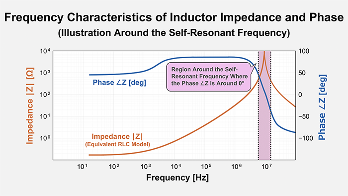
The inductive reactance and capacitive reactance cancel, the phase crosses 0°, and the impedance magnitude ∣Z∣ reaches its maximum. Above this frequency, the parasitic capacitance dominates, and the inductor actually behaves as a capacitor (capacitive impedance and negative phase).
If a DC is superimposed, the operating point on the magnetization curve shifts, and the differential permeability decreases. From the point of view of small-signal measurement, the effective L therefore decreases as the dc bias increases, and the impedance curve shifts accordingly, even for the same part number.
Factors That Influence Measured Impedance
In this section, we focus on factors arising from the intrinsic behavior of capacitors and inductors: frequency, dc bias, ac level, and temperature. Errors due to fixtures, calibration, cabling, and environment are covered later under measurement procedures and environment.
Capacitors
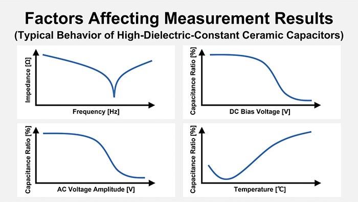
For capacitors, impedance depends strongly on three factors: frequency, dc bias, and temperature. Frequency determines which element of the equivalent circuit dominates? DC bias changes the effective dielectric constant and therefore the apparent capacitance. Temperature changes both capacitance and loss through the dielectric’s temperature coefficient and electrode resistance. In the discussion below, C denotes capacitance, ESR the equivalent series resistance, ESL the equivalent series inductance, and Q the quality factor.
・Frequency dependence
The series-equivalent impedance of a real capacitor can be approximated as
\(Z_s(f)=ESR(f)+\displaystyle\frac{1}{j2πfC}+j2πf\ ESL\)
At frequencies much lower than the self-resonant frequency fSRF, the capacitive term dominates and ∣Z∣ is approximately 1/(2πfC). Near the resonance region, ESR and dielectric loss (often expressed as tanδ) become essential, and the impedance magnitude flattens to a minimum. Above fSRF, the ESL term dominates, and the capacitor appears inductive when observed from the outside.
In practical measurement, the self-resonant frequency is defined as the frequency at which the magnitude ∣Z∣ reaches a minimum and the phase ∠Z crosses 0° when the device is measured at a fixed ac level.
Expressed in series form, Q is
\(Q≈\displaystyle\frac{1}{2πfC\ ESR}\)
Thinking in terms of this formula makes it easier to see intuitively how changes in frequency, ESR, and C affect Q.
・DC bias characteristics
High-dielectric-constant (high-k) multilayer ceramic capacitors, such as X7R and X5R types, show a strong dc-bias effect. When a high DC voltage is applied, the polarization inside the dielectric approaches saturation. The effective dielectric constant decreases, and the measured capacitance decreases with increasing dc bias.
This behavior arises because the relationship between the electric field E and the dielectric permittivity ε is not linear; the permittivity decreases as the electric field increases. Because of this nonlinearity, capacitance comparisons must always be made under matched conditions: the same frequency, the same ac level (typically 0.1–0.5 Vrms; for high-k parts, values around 0.1 Vrms are recommended), the same temperature, and the same dc bias representing expected operating conditions.
・Temperature characteristics
The dielectric’s temperature coefficient causes capacitance and loss to vary with temperature. For ceramic capacitors, typical behaviors are: C0G/NP0 types are almost temperature-independent; X7R devices stay within roughly ±15% over −55 to 125 °C; and Y5V devices exhibit much larger variation and must be used carefully in design.
Evaluation is done at a fixed frequency, sweeping the temperature over the required range. If necessary, you measure both during temperature rise and during temperature fall to check hysteresis.
Inductors
For inductors, three factors significantly affect the measured impedance: frequency, dc bias, and ac excitation level. Frequency determines where self-resonance occurs and whether the behavior is inductive or capacitive. DC bias lowers the small-signal inductance. Excessive AC amplitude pushes the magnetic material into a nonlinear region, increasing loss and decreasing Q.
・Frequency dependence (self-resonance)
The self-resonant frequency fSRF of an inductor is determined mainly by its inductance L and the parasitic inter-winding capacitance CP. To a first approximation,
\(f_{SRF} ≈\displaystyle\frac{1}{2π\sqrt{LC_p}}\)
For frequencies below fSRF, the inductance term dominates; the impedance is inductive, and ∣Z∣ increases approximately in proportion to frequency. As the frequency approaches fSRF, L and CP resonate, the slope of ∣Z∣ and the phase are distorted, and you see ∣Z∣ reach a maximum at the frequency where the phase crosses 0°. Above fSRF, the parasitic capacitance dominates, and the observed impedance becomes capacitive.
The basic behavior of Q is that as frequency rises, RAC(f) increases, so Q = ωL/RAC(f) eventually stops increasing and then falls.
・DC bias characteristics
When a DC flows through the inductor, the operating point on the B–H curve shifts away from the origin. The differential permeability decreases in this region, and the small-signal inductance measured by the ac measurement decreases accordingly.
For accurate comparison, measurements of bias-dependent inductors should be made at low frequency with a small ac signal, at a controlled temperature, and with the dc bias matched to actual operating conditions.
・AC excitation level
If the ac drive amplitude is too large, the measurement no longer reflects the actual small-signal “differential” inductance but instead some average “incremental” inductance over the excursion. This generally appears as a smaller measured L. As the AC amplitude increases, core loss also increases; the equivalent resistance increases, and Q decreases.
The detailed dependence of loss on amplitude varies with material, but for practical design, it is enough to remember that “higher ac flux density leads to higher loss.”
Impedance Measurement Procedures and How to Read the Data
To evaluate components accurately and predict circuit performance, you must not only measure impedance but also understand the procedure and how to interpret the data. If your criteria for judging measured values are vague, the design will not achieve its intended performance. In this section, we walk through typical measurement examples for capacitors and inductors and explain how to read the data.
Finding and Interpreting Self-Resonant Frequency
At the self-resonant frequency of a component, the capacitive reactance and inductive reactance of its equivalent circuit have equal magnitude. The total reactive part is zero, so the impedance phase angle crosses 0°. At the same time, the impedance magnitude ∣Z∣ reaches an extreme value. For capacitors, this extreme is a minimum; for inductors, it is a maximum.
In practical work, you sweep the frequency and plot ∣Z∣ and phase versus frequency. You then confirm that the frequency where ∣Z∣ is minimum (for a capacitor) or maximum (for an inductor) coincides with the frequency where the phase angle passes through 0°. That frequency is defined as the self-resonant frequency fSRF.
For capacitors, behavior above fSRF is inductive due to ESL. For inductors, behavior above fSRF is capacitive due to parasitic capacitance.
Pre-Measurement Calibration: Open–Short–Load Correction and Fixture Management
The automatically balanced bridge method maintains bridge balance automatically using operational amplifier virtual short principles. Typical automatically balanced bridge-type LCR meters operate from 10Hz to 2 MHz (high-frequency models: 1Hz to approximately 120 MHz). Measurements below 1Hz or above 100MHz typically employ alternative methods (I-V method, VNA, etc.). Many impedance meters (LCR meters) adopt this approach with sub-second measurement times suitable for production lines.
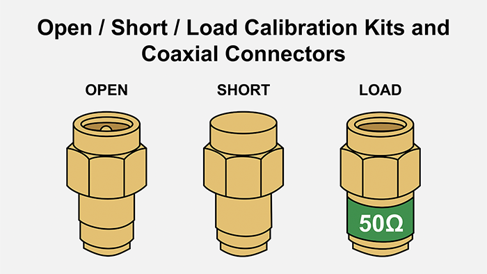
When you perform a one-port (1-port) calibration on a vector network analyzer or high-frequency impedance analyzer, you usually use three calibration standards: Open, Short, and Load (OSL). Each standard is modeled not as an ideal element, but as a perfect element plus its realistic parasitic components.
Open: An open circuit ideally has infinite impedance. In reality, an open at the end of a connector has residual capacitance between conductors due to fringe electric fields. The Open standard is therefore modeled as a large impedance with a specified small capacitance; if needed, higher-order frequency-dependent terms are also added.
Short: Ideally, a short circuit has 0 Ω. In practice, the conductors and joints have unavoidable inductance. The Short standard is modeled as a small inductance in series with a minimal resistance. If the standard or fixture has a finite physical length, delay terms corresponding to the electrical length are added to the model to correct phase errors.
Load: The Load standard is a precision 50 Ω resistor (or 75 Ω, depending on system impedance). Its model includes the slight deviation from exactly 50 Ω and the frequency dependence of that resistance. Because its reflection is small over the specified band, it is used as the reference “matched load” for calibration.
By measuring these three modeled standards at the reference plane of interest, the instrument can estimate its systematic error terms and reconstruct the device under test’s actual reflection coefficient and impedance at that plane.
Calibration procedure
In practical work, calibration is carried out along the following steps. Here, the numbering is for procedure clarity rather than to impose strict order across all instruments.
- Decide on the measurement frequency range and test level, and power on the instrument long enough to stabilize its internal temperature.
- Clean and inspect the test port and fixture. Verify that there is no contamination or mechanical damage to the center conductor or dielectric.
- Connect the Open standard at the actual fixture plane and perform the Open calibration step. The instrument effectively records the stray capacitance at the open terminals (typically 0.05–0.2 pF).
- Connect the Short standard at the same plane and perform the Short calibration step. The instrument records the residual inductance (typically 0.1–1 nH).
- Connect the Load standard and perform the Load calibration step. The instrument records the standard’s effective resistance and phase at each frequency.
- If necessary, apply fixture-specific corrections such as de-embedding or electrical extension so that the final reference plane coincides with the intended measurement plane on the device under test.
- Immediately after calibration, measure a known component, such as a precision resistor or capacitor, to verify that the estimated value agrees with its known value within the expected tolerance.
- Record the calibration conditions (frequency range, test level, averaging, temperature, humidity, and the specific standards used) so that the calibration can be reproduced later. For long test sessions or when the environment changes, insert short verification measurements at regular intervals and recalibrate if drift is observed.
Coaxial connector characteristics
Coaxial connectors themselves are specified by characteristic impedance, typically 50 Ω (or 75 Ω for some video or broadband applications). In reality, the matching quality is not defined by a simple resistance tolerance, but by VSWR (Voltage Standing Wave Ratio) or return loss (RL) as a function of frequency. Because the reflection coefficient depends on frequency, you must consult the data sheet curves for VSWR or RL across the relevant band when selecting connectors.
Insertion loss is likewise frequency-dependent and depends on geometry, material, surface finish, and the connector’s mounting. Therefore, always refer to the part-specific band-by-band specifications rather than assuming generic values.
Verification after calibration
After calibration, it is good practice to confirm the calibration state using one or more check standards. For example, you can connect a 100 Ω ±0.1% precision resistor and verify that the measured value is within ±0.2%. This simple check, performed daily or at the start of each measurement session, helps catch problems such as damaged cables, degraded connectors, or misapplied calibration data.
Measuring Capacitors: Procedures for Evaluating Capacitance and ESR
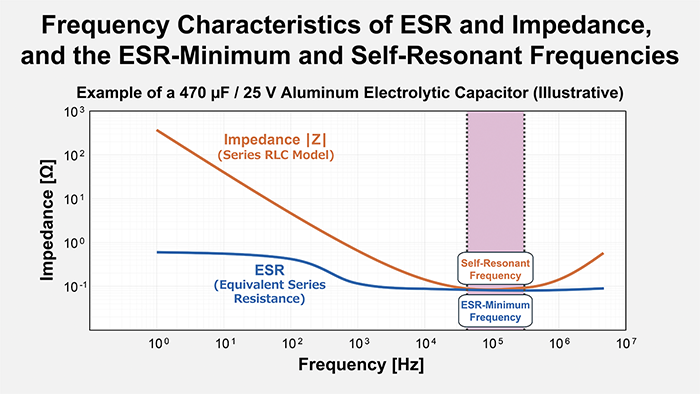
For capacitors, you usually want to evaluate capacitance, ESR, and loss angle tanδ, so that you can predict both frequency response and power loss in the circuit. In aluminum electrolytic capacitors, ESR at 100 kHz can range from tens of milliohms to several ohms, and this has a strong influence on ripple current capability and noise filtering.
Measurement procedure and decision criteria
Before measuring, you confirm the initial state: check for discoloration, swelling, or leakage, and ensure any residual DC voltage between the terminals has been discharged.
For basic characteristics, measurements are often made at 120 Hz for aluminum electrolytic capacitors and at 1 kHz for general ceramic capacitors. A typical signal level is 0.5 Vrms or lower, starting with no DC bias applied.
To evaluate frequency characteristics, you sweep the frequency and record capacitance, ESR, and loss. A typical set of frequencies and evaluation items is as follows.
| Frequency | Primary evaluation items | Impact on design |
|---|---|---|
| 120 Hz | Capacitance, tanδ | Basic catalog characteristic |
| 1 kHz | ESR, capacitance | Standard evaluation point |
| 10 kHz | ESR trend change | For switching applications |
| 100 kHz | Minimum ESR | High-frequency performance |
| ≥ 1 MHz | Start of ESL influence | Self-resonant behavior check |
| Frequency | Capacitance | ESR | tanδ | Notes |
|---|---|---|---|---|
| 120Hz | 485µF | 0.58Ω | 0.21 | Within spec |
| 1kHz | 478µF | 0.35Ω | 1.05 | Typical |
| 10kHz | 472µF | 0.12Ω | 3.55 | ESR lowering |
| 100kHz | 465µF | 0.085Ω | 25.0 | Optimum |
From the ESR at 100 kHz, you can estimate ripple-current heating. The basic relation is
\(P_{loss}=I_{rms}^2×ESR\)
If the allowable ripple current is 1 Arms and ESR = 0.085 Ω at 100 kHz, then
\(P_{loss}=1^{2}×0.085=0.085\)
Assuming a thermal resistance of 10 °C/W, the temperature rise is about
\(ΔT≈10℃/W×0.085 W=0.85℃\)
This kind of estimate allows you to check whether the ripple current ratings and the thermal design have sufficient margins.
The frequency dependence of ESR in aluminum electrolytic capacitors reflects several mechanisms. At low frequency, the electrolyte resistance dominates. In the mid-frequency range, a combination of electrolyte and aluminum foil resistance shapes the curve. At high frequency, skin effect increases the effective resistance of the foil, and ESR eventually rises again.
Measuring capacitor self-resonance
At the self-resonant frequency, the magnitudes of capacitive and inductive reactance are equal:
\(|X_C |=|X_L |\)
This is the same condition used earlier to derive fSRF. In practice, you
- Sweep frequency and identify the frequency where the impedance magnitude ∣Z∣ is minimum.
- Confirm that at the same frequency, the phase angle is near 0°.
- Check that above this frequency, the behavior becomes inductive (positive phase).
If these conditions are satisfied, you can treat that frequency as the self-resonant frequency for design purposes.
Measuring Inductors: Self-Resonant Frequency and AC Resistance (ACR)
For inductors, it is essential to confirm the frequency range over which the designed inductive behavior is maintained. Above the self-resonant frequency, the inductor behaves as a capacitive element, and the assumptions used in the design no longer hold. The frequency dependence of the ac resistance RAC(f) is directly tied to power loss.
Measurement procedure
For basic characteristics, you typically measure at the instrument’s default frequency, often 1 kHz, with a trim AC level, such as 0.1 Vrms, to avoid saturation. Record inductance L and quality factor Q under these conditions.
To evaluate frequency characteristics, you sweep the frequency, for example, from 100 Hz up to ten times the expected self-resonant frequency. At each point, you record L, Q, RAC(f), and phase.
To identify the self-resonant point, you look for the frequency at which
- The impedance magnitude ∣Z∣ reaches a maximum, and
- The phase angle crosses 0°
and confirm that these two frequencies coincide within measurement uncertainty.
Frequency dependence of AC resistance
The frequency dependence of winding resistance arises from several effects: the skin effect, the proximity effect (distortion of the current distribution due to adjacent conductors), and eddy-current losses in the magnetic core. As a simple model, the ac resistance can be approximated as
\(R_{AC}(f)=R_{DC}\sqrt{\displaystyle\frac{f}{f_0}}\)
where f0 is the frequency at which skin effect becomes significant. From measured inductance and Q, RAC(f) can also be estimated as
\(R_{AC}(f)=\displaystyle\frac{2πfL}{Q}\)
Example: Evaluating a power inductor
Consider a power inductor with nominal specifications L = 47 µH, rated current 3 A, ferrite core. At 1 kHz and small-signal conditions, the measurement gives
- Inductance L = 46.8 μH
- Q = 45
From this, you can estimate
\(R_{AC}(f)=\displaystyle\frac{2πfL}{Q}=\displaystyle\frac{2π×1000×46.8×10^{\ -6}}{45}=6.5mΩ\)
At the rated current of 3 A, the power loss is
\(P=3^{2}×0.0065=58.5mW\)
If the thermal resistance is roughly 100 °C/W, the temperature rise due to this loss alone is about
\(ΔT≈100℃/W×0.0585 W≈5.9℃\)
Example: Measuring inductor self-resonance
Suppose you measure a 1210-size 10 µH chip inductor and obtain the following data:
| Frequency | Impedance magnitude | Phase angle | Notes |
|---|---|---|---|
| 1MHz | 62.8Ω | +89° | Inductive |
| 5MHz | 314Ω | +88° | Inductive |
| 15MHz | 485Ω | +45° | Near resonance |
| 18MHz | 534Ω | 0° | Self resonance |
| 25MHz | 398Ω | -45° | Capacitive |
From these measurements, the self-resonant frequency is about 18 MHz. You can estimate the parasitic capacitance using.
\(C_p=\displaystyle\frac{1}{(2πf_{SRF})^2 L}\)
Substituting fSRF = 18 MHz and L = 10 gives
\(C_p=\displaystyle\frac{1}{(2πf_{SRF})^2 L}=\displaystyle\frac{1}{(2π×18×10^{\ 6})^2×10×10^{-6}}\ \ \ =7.8pF\)
If the parasitic capacitance estimated from measurement differs significantly from that implied by the device’s data sheet or by other measurements, it is a signal to recheck both the SRF measurement and the inductance value.
Key Points for Improving Measurement Accuracy
Overall measurement accuracy is determined primarily by calibration procedures and environmental conditions. Poor calibration alone can easily introduce errors exceeding ±10%, which directly affects product acceptance testing and margin analysis.
In this section, we look at how to set measurement conditions and how to control the measurement environment to suppress errors.
Setting Measurement Conditions: Frequency and Signal Level
Both measurement frequency and signal level directly affect accuracy. As a basic rule, you should measure at or near the actual operating frequency of the component. When you also need to understand broadband behavior, it is common to perform a logarithmic frequency sweep.
Choosing measurement frequency and sweep settings
The table below summarizes typical standard measurement frequencies and additional evaluation frequencies for each component type.
| Component type | Standard measurement frequency | Additional evaluation frequencies |
|---|---|---|
| Aluminum electrolytic capacitor | 120Hz, 1kHz | 10kHz, 100kHz |
| Ceramic capacitor | 1kHz, 1MHz | Self-resonant frequency |
| Inductor | Instrument standard (often 1 kHz) | Self-resonant frequency |
| Resistor | 1kHz | Ten times the intended operating frequency |
For a sweep, a typical setting is:
- Start frequency: 1 Hz or 10 Hz
- Stop frequency: about ten times the component’s self-resonant frequency
- Number of points: about 10 points per decade of frequency
This provides sufficient resolution to identify resonance and loss changes without generating excessive data volume.
Optimizing signal level
The measurement ac level must be chosen to satisfy both noise and linearity constraints. Three factors are especially important.
First, the thermal noise level is set by the well-known Johnson–Nyquist relation
\(V_{noise}=\sqrt{4kTRB}\)
where k is Boltzmann’s constant, T is absolute temperature, R is resistance, and B is measurement bandwidth.
Second, you must avoid driving the device into nonlinear behavior. For ceramic capacitors, excessive AC level changes the apparent capacitance because the dielectric is nonlinear. For inductors, large AC amplitudes move the operating point on the B–H curve and change both L and loss.
Third, the signal must be sufficiently larger than the noise to achieve the desired resolution. The signal-to-noise ratio (SNR) in decibels is
\(SNR=20 {log}_{10}\left(\displaystyle\frac{V_{signal}}{V_{noise}}\right)\)
As a rule of thumb, to achieve 0.1% accuracy, you need an SNR greater than about 60 dB, that is, a signal 1000 times larger than the noise.
For a practical example, consider measuring a 1 MΩ resistor with a measurement bandwidth of 1 kHz at room temperature (about 25 °C). The thermal noise is approximately 4.0 µVrms. To get 60 dB SNR, the signal must be at least 4.0 mVrms. In practice, a measurement signal level in the range 10–50 mVrms provides margin while keeping power dissipation small.
For many component measurements, a recommended range is 0.1–1 Vrms. High-k ceramic capacitors should generally be measured at the lower end of this range (around 0.1 Vrms) to avoid bias-dependent effects unless those effects are intentionally being characterized.
Controlling the Measurement Environment: Temperature, Humidity, and Parasitics
Managing the measurement environment is essential for mitigating errors caused by temperature and humidity changes and parasitic elements. Temperature drift can alter the instrument’s internal calibration. Humidity changes insulation resistance. Cable and fixture parasitics, as well as external noise, can compromise repeatability and long-term stability.
Temperature control
The temperature stability of the measuring instrument is determined by the temperature coefficients of its internal reference elements. Typical values are:
- Precision resistors: approximately ±1–5 ppm/°C
- Reference voltage sources: approximately ±1–3 ppm/°C
- Crystal oscillators: approximately ±0.1–1 ppm/°C
A ±1 °C temperature change thus causes a relative error of 1–5 ppm (0.0001–0.0005%). Even in stricter configurations, taking 10 ppm (0.001%) as a practical upper bound per 1 °C temperature change is usually safe.
Practical temperature control techniques include using a constant-temperature chamber with ±0.5 °C control, ensuring the instrument has sufficient warm-up time (30 minutes or more), and thermal shielding to reduce the effect of room temperature changes.
Humidity effects and countermeasures
In high-impedance measurements, humidity significantly affects insulation resistance. The humidity dependence can be expressed qualitatively by an exponential relation such as
\(log(R_{ins})=A-B×RH\)
where A and B are material constants, and RH is relative humidity in percent. As humidity rises, leakage currents increase, and apparent impedance decreases. The sensitivity of resistance to humidity changes also depends heavily on the material used, so it is essential to know the material characteristics when evaluating high-impedance components.
Common countermeasures include controlling the laboratory to 40–60% relative humidity, using nitrogen purging inside the measurement chamber for very high-impedance measurements, and placing desiccants, such as silica gel, near critical fixtures.
Parasitic elements in cables and fixtures
Cables and fixtures always introduce parasitic elements. Their influence is enormous when the device under test has high impedance. A typical 50 Ω coaxial cable has a distributed capacitance of roughly 100 pF/m. If you connect several meters of cable to a gigaohm-level device, the cable capacitance dominates unless compensated.
To minimize these effects, you should keep cables as short as possible, perform open- and short-circuit compensation at the actual fixture, and use guarding and shielding properly. Guarding can reduce leakage paths across insulators, and shielding reduces sensitivity to external electric fields and noise.
Types of Impedance Measurement Methods and How to Choose Among Them
Impedance measurement methods can be classified by their measurement principle and applicable frequency range. From classical bridge methods to modern S-parameter techniques, several approaches exist, each with its own strengths in terms of accuracy, frequency coverage, and ease of use.
The table below summarizes typical application ranges and recommended methods.
| Approximate frequency band | Typical impedance range | Recommended method | Main purpose |
|---|---|---|---|
| 10 Hz – 2 MHz (up to ~120 MHz for some models) |
1 mΩ – 100 GΩ | Automatically balanced bridge (LCR meter) | General evaluation of C, L, R and loss |
| 10 kHz – 100 MHz | 1 Ω – 10 kΩ | High-frequency LCR | High-frequency characteristics of passive parts |
| Several MHz – several GHz | 1 Ω – 10 kΩ (non-50 Ω region) | RF I–V method | Absolute impedance of non-50 Ω devices |
| 100 MHz – several GHz | Around 50 Ω | S-parameter method (VNA) | Relative measurement and modeling of 50 Ω systems |
| ≤ 1 kHz (highest accuracy) | Arbitrary (relative to a standard) | Classical bridge | Highest-accuracy standard comparisons |
Below, we outline the characteristics of each method.
Bridge Method: High Precision but Slow and Low-Frequency
The classical bridge method compares an unknown impedance with known standards under a balance condition. In principle, if the standard has an accuracy of ±0.01%, the unknown impedance can be measured with an overall accuracy of ±0.1%. However, the balance point must be determined by manually adjusting elements, which takes time and skill, so individual measurements often require several minutes.
Because the bridge circuitry itself is complex to realize at high frequencies and the method is relatively slow, it is mainly used below about 1 kHz for calibrating standards and performing the highest-accuracy comparisons at metrology laboratories.
Automatically Balanced Bridge Method: Standard Wideband Method (1 Hz – 120 MHz)
Modern LCR meters use the automatically balanced bridge method, which exploits the virtual-short property of operational amplifiers to maintain bridge balance automatically. Typical general-purpose LCR meters cover roughly 10 Hz to 2 MHz; high-frequency LCR meters extend this up to around 120 MHz. For frequencies below 1 Hz or above 100 MHz, other methods, such as dc techniques, I–V methods, or S-parameter measurements, are usually used instead.
Because the bridge is balanced automatically, measurement time is short (often less than 1 second), making this method suitable for both bench evaluation and production-line testing of capacitors, inductors, and resistors.
Basic I–V Method: Simple Impedance Measurement with a Current-Sense Resistor
In the I–V method, you apply an AC signal to the device under test and calculate its impedance from the ratio of the voltage to the current. The current is measured using a shunt resistor, so the fundamental relation is
\(Z_x=\displaystyle\frac{V_x}{I_x} =R_s\displaystyle\frac{V_x}{V_s}\)
where Zx is the device under test, Rs is the shunt resistor, and Vx and Vs are the voltages across the device and the shunt resistor, respectively.
Because this method uses a simple circuit configuration, it is easy to implement with general lab instruments such as function generators and oscilloscopes. The principle is clear, and it is easy to adapt to special conditions such as DC biasing or large currents. On the other hand, the accuracy of the impedance value depends directly on the shunt resistor’s precision and frequency characteristics, so selecting and calibrating the shunt is critical.
RF I–V Method: For High-Frequency Measurements from Several MHz to Several GHz
The RF I–V method extends the I–V principle to the RF and microwave region. It helps measure absolute impedance in the multi-MHz to multi-GHz band when the device is not well matched to the standard 50 Ω of most RF equipment. Typical applications include measuring chip inductors, chip capacitors, and non-50 Ω devices at VHF, UHF, and microwave frequencies.
Because parasitic effects from the measurement system become large at these frequencies, RF I–V setups use coaxial structures, baluns, and careful calibration. Calibration follows the same basic Open–Short–Load concept as VNAs, and specialized fixtures are often required. Expertise in RF measurement is needed to correctly build and interpret the setup.
S-Parameter Method (VNA): Applying Characteristic Impedance for High-Frequency Measurement
The S-parameter method uses a vector network analyzer referenced to a characteristic impedance (typically 50 Ω or 75 Ω). Rather than measuring current and voltage directly, the VNA measures scattering parameters that describe how incident waves are reflected and transmitted.
For a one-port measurement, the key quantity is S11 (the reflection coefficient):
\(S_{11}=\displaystyle\frac{V^-}{V^+}=\displaystyle\frac{Z_x-Z_0}{Z_x+Z_0}\)
where Zx is the impedance of the device under test and Z0 is the characteristic impedance of the system. From S11, you can recover the impedance as
\(Z_x=Z_0\displaystyle\frac{1+S_{11}}{1-S_{11}}\)
This method is the mainstream approach in the multi-GHz region for antennas, RF circuits, and high-speed digital interconnects. Results are often visualized on a Smith chart by plotting the normalized impedance z = Zx/Z0.
By combining S-parameter measurements with fixture de-embedding, you can build accurate high-frequency models of components and interconnects referenced to a specific plane, and then use those models in simulation and design.
Summary of Impedance Measurement
In impedance measurement, the first step is to choose an appropriate measurement method based on the frequency band and the measurement purpose. For low- to mid-frequency evaluation of passive components, automatically balanced-bridge LCR meters are convenient and widely used. In high-frequency bands, it is often more practical to obtain impedance indirectly via reflection measurements using a vector network analyzer.
Regardless of method, accurate calibration is essential. You must minimize the parasitic elements introduced by fixturing and leads, and adjust environmental conditions such as temperature, humidity, and external noise. The measurement frequency should match the intended operating frequency, and the signal level should be set high enough to achieve the required SNR while remaining low enough to avoid nonlinear device behavior. Always record the conditions used (frequency, amplitude, dc bias, temperature, and humidity) so that measurements can be reproduced and compared.
When evaluating measurement results, you sweep the frequency to identify self-resonant frequencies, then read the component behavior from the relationship between the phase crossing 0° and the extremum of∣Z∣ Capacitors reach a minimum impedance at self-resonance and then exhibit inductive behavior at higher frequencies due to ESL. Inductors reach a maximum impedance at self-resonance, then exhibit capacitive behavior at higher frequencies due to parasitic capacitance. At the same time, you examine the quality factor Q and loss indicators, such as ESR or ac resistance, to estimate heating margins and usable bandwidth.
Finally, if you standardize notation and assumptions within your organization —for example, how frequency is written, how loss resistances are defined and symbolized, and which equivalent circuits are used—then measured impedance data can be fed directly into design calculations without confusion. By consistently applying these practices, you can integrate measurement, evaluation, and design decisions smoothly and build more reliable circuits with fewer iterations.
Related article
What is Impedance? AC Circuit Analysis and Design
【Download Documents】 AC Circuit Fundamentals
This handbook summarizes key AC circuit concepts from each article, including reactance, impedance, resonance, power, and power factor. It outlines derivations and circuit behavior, highlighting essential ideas for circuit design.

Electrical Circuit Design
Basic
- Seven Tools for Soldering
- Soldering Techniques and Solder Types
- Seven Techniques for Printed Circuit Board Reworking
-
AC Circuits Fundamentals: Article Guide
- AC Circuits: Alternating Current, Waveforms, and Formulas
- Complex Numbers in AC Circuit
- Fundamentals of Capacitive Circuits: Understanding Series and Parallel Capacitor Connections
- Electrical Reactance
- What is Impedance? AC Circuit Analysis and Design
- Impedance Measurement: How to Choose Methods and Improve Accuracy
- Impedance Matching: Why It Matters for Power Transfer and Signal Reflections
- Resonant Circuits: Resonant Frequency and Q Factor
- RLC Circuit: Series and Parallel, Applied circuits
- What is AC Power? Active Power, Reactive Power, Apparent Power
- Power Factor: Calculation and Efficiency Improvement
- What is PFC?
- Boundary Current Mode (BCM) PFC: Examples of Efficiency Improvement Using Diodes
- Continuous Current Mode (CCM) PFC: Examples of Efficiency Improvement Using Diode
- LED Illumination Circuits:Example of Efficiency Improvement and Noise Reduction Using MOSFETs
- PFC Circuits for Air Conditioners:Example of Efficiency Improvement Using MOSFETs and Diodes
-
DC Circuits Fundamentals: Article Guide
- Electric Current and Voltage in DC Circuits
- Ohm’s Law: Voltage, Current, and Resistance
- Kirchhoff’s Circuit Laws
- What Is Mesh Analysis (Mesh Current Method)?
- What Is Nodal Analysis (Nodal Voltage Analysis)?
- Thevenin’s Theorem: DC Circuit Analysis
- Norton’s Theorem: Equivalent Circuit Analysis
- What Is the Superposition Theorem?
- What Is the Δ–Y Transformation (Y–Δ Transformation)?
- Voltage Divider Circuit
- Current Divider and the Current Divider Rule