Transistors|Basic
NPN Transistor: Low-Side Switch Fundamentals
2026.02.27
table of contents
- ・Role and Applications of NPN Bipolar Junction Transistors
- ・NPN Transistor Low-Side Wiring (Verify Basic Configuration with Diagrams)
- ・Conditions for Proper NPN Switch Operation (Cutoff and Saturation)
- ・Protection and Wiring Techniques (Stabilizing NPN Transistors in Low-Side Operation)
- ・Common Low-Side Problems and Remedies
- ・Summary
An NPN bipolar junction transistor is an electronic component that allows a small base current to control a much larger collector-to-emitter current. When used as a low-side (sink) switch, an NPN transistor enables microcontroller or logic IC outputs to drive loads such as LEDs, relays, and small motors. Stable low-side operation is achieved only when four conditions are satisfied: the current path sequence is correct, the saturation conditions are met, inductive loads are protected against back EMF, and the base node is kept at a defined potential (i.e., it is not left floating) when the drive output is inactive.
All circuit diagrams in this article use the common-emitter configuration. We focus on the relationship between collector–emitter voltage (VCE) and collector current (IC) from the standpoint of switching operation, while explaining wiring order, operating conditions, and typical problems and their remedies. Field-effect transistors control channel conduction by applying an electric field. In contrast, bipolar junction transistors (BJTs) rely on transistor action driven by diffusion and recombination of electrons and holes as mobile charge carriers.
Role and Applications of NPN Bipolar Junction Transistors
An NPN transistor operates as a current amplifier: by driving a small base current, it enables a large collector-emitter current to flow. Typical microcontroller output pins can source/sink only a few to a few tens of milliamps directly. However, if you use this limited current as base drive and a suitable transistor is selected, the collector–emitter path of the NPN transistor can switch load currents in the several-hundred-milliamp range, up to around 1 A depending on the application.
Understanding how NPN devices differ from PNP transistors and high-side configurations is essential when selecting an appropriate circuit topology. Using its DC gain (hFE), the NPN bipolar transistor uses a small base current to control the collector current (detailed design aspects are discussed in separate articles).
Why NPN Devices Are Used in Low-Side Switches
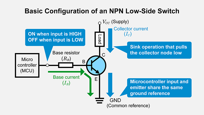
The key advantage of using NPN transistors in a low-side configuration is that the base can be driven directly from a microcontroller or logic IC output, referenced to a common ground. Because the emitter is tied to the same ground as the microcontroller, the GPIO high level drives the base through RB. When the transistor turns on, the base is clamped at about VBE (≈0.7–0.9 V), and the remaining voltage (VGPIO − VBE) appears across RB to set IB.
When the output pin is at a high logic level (e.g., 3.3 V or 5 V), the NPN transistor turns on and sinks load current to ground. When the output pin is low (0 V), the base–emitter junction is no longer forward-biased, and the transistor turns off.
For example, consider driving a 5 V, 70 mA relay with a general-purpose NPN transistor. If we choose a forced β of 10, the required base current becomes:
IB ≈ 70 mA / 10 = 7 mA
Before finalizing RB , confirm that the GPIO can source this IB while meeting its guaranteed VOH; if VOH drops at the required current, use VOH (min) (not the nominal 3.3 V/5 V) in the RB calculation.
For a 3.3 V GPIO output, the base resistor can be estimated as:
RB ≈ (3.3 − 0.7) / 0.007 ≈ 370 Ω
For a 5.0 V output, the estimate becomes:
RB ≈ (5.0 − 0.7) / 0.007 ≈ 610 Ω
Design note: After selecting a standard RB value, re-check that IB is still sufficient, since VBE in saturation can be higher than 0.7 V.
If VCE(sat) is about 0.2 V at the operating current, the device power dissipation is approximately:
P ≈ 0.2 × 0.07 = 14 mW
In high-side configurations, when the load supply voltage differs from the microcontroller supply, level-shift circuits or detailed voltage calculations are required. Even with equal supply voltages, PNP transistors need inverted logic control. From the microcontroller’s perspective, low-side NPN switching simplifies the drive circuitry because little or no level shifting is needed and logic levels can be applied directly.
For a comprehensive overview of bipolar junction transistors, see Bipolar Junction Transistor (BJT) Basics: Operation and Applications (NPN & PNP).
Key Differences Between NPN and PNP in High-Side and Low-Side Roles
The differences between NPN and PNP transistors appear in both current direction and the polarity of the control voltage. If the emitter connection is wrong, the transistor may fail to turn off properly or even be damaged by reverse biasing.
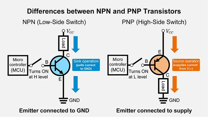
In low-side switching, an NPN transistor acts as a current sink, pulling the node low. In high-side switching, a PNP transistor serves as a source: it supplies current from the positive supply to the load.
In low-side applications, the NPN emitter must be tied to ground. In high-side PNP applications, the emitter must be connected to the positive supply. Reversing these emitter connections can cause leakage current to flow even when the transistor is intended to be off.
Once these polarity and current-direction differences are understood, the designer can decide whether a high-side or low-side topology is more appropriate. In an NPN switch, conventional current enters the collector and leaves the emitter. In a PNP high-side switch, it enters the emitter and leaves the collector. The control polarity is also inverted.
NPN Transistor Low-Side Wiring (Verify Basic Configuration with Diagrams)
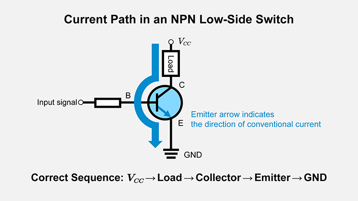
The most common cause of malfunction in low-side wiring is an incorrect current path. In a correctly wired circuit, current flows in the following sequence:
Supply (VCC) → Load → Collector → Emitter → Ground
In this article, VCC denotes the positive supply connected to the load (the load supply), which may be different from the microcontroller supply.
If any connection in this sequence is reversed, the transistor may fail to conduct or be subjected to reverse bias, which can cause damage.
The emitter arrow in the transistor symbol indicates the direction of conventional current. Paying attention to the emitter arrow orientation helps prevent polarity errors. In open-collector configurations, the load is connected to the supply side, and the transistor pulls the load node down to ground.
The basic low-side circuit with a resistive load clearly shows the positional relationship among the supply voltage, load, and the collector node (which also serves as the output node). Structurally, an NPN transistor consists of a thin p-type base region sandwiched between two n-type regions. The emitter is typically heavily doped, the base is lightly doped, and the collector has an intermediate doping level. These structural differences are reflected in the rated voltages and current capabilities for each terminal.
Circuit Sequence and Preventing Polarity Errors Using Symbol Arrows
When the NPN transistor is on, current enters through the collector, passes through the emitter, and returns to ground, driving the load. When the transistor is off, the base current is essentially zero, and the collector-to-emitter path is cut off.
Circuit Sequence and Current Path (VCC → Load → NPN → GND)
If this sequence is disrupted, device characteristics degrade sharply, and the risk of damage increases. Collector–emitter reverse connection is an unintended operating mode in which the reverse-mode gain is orders of magnitude lower than the forward-mode β, and even the voltage ratings may not be guaranteed. Such a reversed connection is not recommended, even for temporary evaluation wiring. Calculation methods for base resistor and collector current design are discussed in the companion article on NPN transistor switching design.
Preventing Polarity Errors Using Symbol Arrows
In schematic symbols for NPN transistors, the emitter arrow points outward, away from the transistor body. This arrow indicates the direction of conventional current: outward for NPN devices and inward for PNP devices. The arrow is used solely to distinguish polarity and does not indicate which terminal connects to ground.
Carefully confirming the arrow direction in the symbol prevents confusion between NPN and PNP transistors and helps avoid swapping collector and emitter connections. Detailed definitions of transistor symbols and terminal naming conventions are covered in the article on Bipolar Junction Transistor (BJT) Basics: Operation and Applications (NPN & PNP).
Open-Collector Wiring Considerations
In an open-collector configuration, the collector node is used as the output, and an external element connected to +V—either a pull-up resistor (logic signaling) or a load (power switching)—is placed between the positive supply (VCC) and the NPN transistor’s collector. When the transistor turns on, the collector voltage falls to approximately VCE(sat), allowing current to flow through the load. When the transistor is off, the collector node becomes high impedance, and the load current drops to nearly zero.
In practice, however, a small leakage current flows even when the transistor is off. This leakage is specified as ICEO or ICEX in datasheets. Because leakage currents increase with temperature, designers must define a threshold current below which the output is still treated as “high impedance” or “OFF.” Off-state leakage appears in the output characteristics, so checking specifications under reverse-biased conditions is essential.
Open-collector stages are often used in two common ways: as logic-level open-collector outputs, and as low-side switches for DC loads. For logic-level open-collector outputs, an external pull-up resistor to VCC defines the HIGH level when the transistor is off; its value trades off static current (when LOW) against rise time. For low-side switching of DC loads (for example, a relay coil, or an LED with a series current-limiting resistor), the load itself provides the path to VCC and sets the load current, so a separate pull-up resistor is usually not required. Practical pull-up value selection is treated in a separate article. For actual component selection during implementation, see the articles on load switch design and digital transistor (RET) selection.
Conditions for Proper NPN Switch Operation (Cutoff and Saturation)
Whether an NPN transistor behaves as a proper switch depends on whether its operating point alternates only between cutoff and saturation.
In the cutoff state, the base–emitter junction is not sufficiently forward-biased, and the collector current is nearly zero. In the saturation state, the collector–emitter voltage VCE drops to VCE(sat), and the effective resistance between the collector and emitter becomes minimal. In this state, the transistor behaves like a closed mechanical switch.
If the transistor remains in the intermediate active region between cutoff and saturation, a significant voltage drop occurs across the collector–emitter path, increasing heat generation and potentially leading to malfunction or device failure. In the active region, the base–emitter junction is forward-biased, while under most operating conditions, the collector–base junction remains reverse-biased. In this article, we focus on switch designs that avoid dwelling in the active region.
Understanding how VBE, VCE(sat), and IC are related enables us to establish clear, verifiable design conditions. Detailed explanations of dynamic load lines, Q-points, and input/output characteristics in the active region are provided in separate amplifier-design articles.
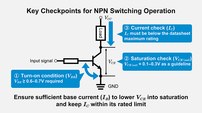
Key Parameters: VBE, VCE(sat), and IC
For switching applications, three parameters determine whether the operation is acceptable: VBE, VCE(sat), and IC. These serve as practical criteria for distinguishing between cutoff and saturation. The combination of applied voltage and load resistance determines the output voltage and current. When the transistor is driven into saturation as intended, VCE drops to a small value, approaching that of a closed switch.
At room temperature, for small-signal transistors operating with collector currents up to roughly 100 mA, the base–emitter voltage at which the base current begins to rise to a practical level is typically taken to be about 0.6–0.7 V. The temperature coefficient is approximately −2 mV/°C. Without securing this forward-bias voltage and the corresponding base current, the transistor does not turn fully on.
The saturation voltage VCE(sat) depends on the device and current conditions. For small-signal operation, values around 0.1–0.3 V are a reasonable guideline. If the measured VCE under “ON” conditions is close to 1 V, the device is not in saturation.
The collector current IC is the current flowing through the load when the transistor is on. The measured value must not exceed the maximum ratings given in the datasheet.
Designing to Avoid Active Region Operation
When the base current is insufficient, the transistor operates in an intermediate state between cutoff and saturation, that is, in the active region. In this state, a significant voltage develops across the collector–emitter path, leading to increased power dissipation. The resulting heat can cause the transistor to malfunction or suffer permanent damage.
Providing a sufficient margin in the base drive ensures that the transistor reliably enters saturation. One helpful concept is forced beta (βforced). Datasheet hFE (DC gain) values are usually measured in the active region. In saturation, the effective gain is lower due to the influence of the base–emitter voltage and internal resistances.
Therefore, designing the base current as IB = IC / hFE, with hFE taken directly from the datasheet, places the operating point near the boundary between saturation and the active region, which is not safe when temperature variations and device-to-device tolerances are considered. Instead, designers typically assume a forced β much smaller than the nominal hFE, for example, βforced ≈ 10–20, and choose base current accordingly.
If a transistor has a nominal hFE around 100, then designing for IB ≈ IC / 10 is a practical rule of thumb for switching use, ensuring saturation with an adequate margin.
Protection and Wiring Techniques (Stabilizing NPN Transistors in Low-Side Operation)
In circuits that drive inductive loads, improper handling of back EMF at switch-off can destroy transistors. When a relay, motor, or solenoid is turned off, the collapsing magnetic field generates a voltage spike. If this voltage exceeds the transistor’s rated voltage, the collector–emitter junction can be punctured, permanently damaging it.
Placing a flyback (freewheel, flywheel) diode in parallel with the load provides a path for the inductive current to recirculate at turn-off, dissipating the stored energy while clamping the voltage and protecting the transistor.
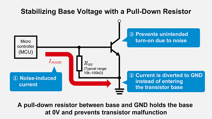
Another critical point is to prevent the base from being left floating. When the base node is floating—that is, not firmly tied to any potential and therefore having an undefined voltage—noise can easily drive the transistor into partial or complete conduction, causing unintended operation. Adding a pull-down resistor from base to ground stabilizes the base potential.
Finally, the routing of the ground return path must be considered. Short, low-impedance ground-return paths improve noise immunity. Long or shared return paths with other high-current lines can introduce common impedance, leading to voltage drops and noise coupling that upset transistor operation.
Darlington configurations can be used when higher current gain is required, but they introduce trade-offs such as increased VCE(sat) and slower switching. These trade-offs need to be evaluated for the specific application.
Flyback Diodes Are Essential for Relays and Motors
In circuits driving inductive loads such as relays, motors, and solenoids, back EMF is generated when the transistor is switched off. When this spike exceeds the transistor’s voltage rating, the collector–emitter junction can break down.
A flyback diode is therefore connected in parallel with the load, with its cathode toward the positive supply (VCC) and its anode toward the transistor (ground side). When the transistor turns off, the current that had been flowing through the load continues to flow, but now circulates through the diode loop. The stored energy in the magnetic field is dissipated gradually, and the voltage across the transistor is clamped, limiting the flyback (back EMF) spike.
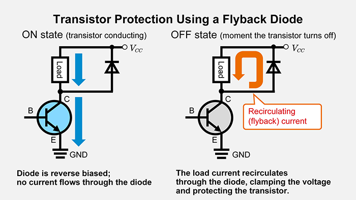
Although the diode suppresses overvoltage, it also slows current decay, which delays the relay’s release timing. When a very fast current cutoff is required, options such as series-connected Zener diodes or RC snubber circuits can be considered. Circuits without any protective element may fail on the first switching operation, depending on the magnitude of the back EMF relative to the device’s voltage rating.
Preventing Base Floating and Routing the Ground Return
When a microcontroller output pin enters a high-impedance state—for example, during startup or reset—the NPN base can be left floating, potentially causing the transistor to malfunction. In such a floating condition, noise makes the base potential undefined, and the load may turn on at unintended times.
Placing a pull-down resistor between the base and ground, typically 10 kΩ to 100 kΩ, keeps the base potential close to 0 V when the driving pin is inactive. The optimal resistor value depends on the driving device and the noise environment.
The ground return path is the route by which current returns from the load and transistor back to the negative terminal of the power supply via the PCB ground plane or ground wiring. In the low-side circuits discussed here, the path “Load → NPN emitter → PCB ground → power supply negative” forms the ground return.
If the trace from the emitter to the PCB ground is long or shares impedance with other large current paths, noise voltages can be induced, resulting in malfunctions. Connecting the emitter to the ground plane with the shortest, widest possible trace and avoiding unnecessary shared impedance with other circuits improves noise immunity.
Common Low-Side Problems and Remedies
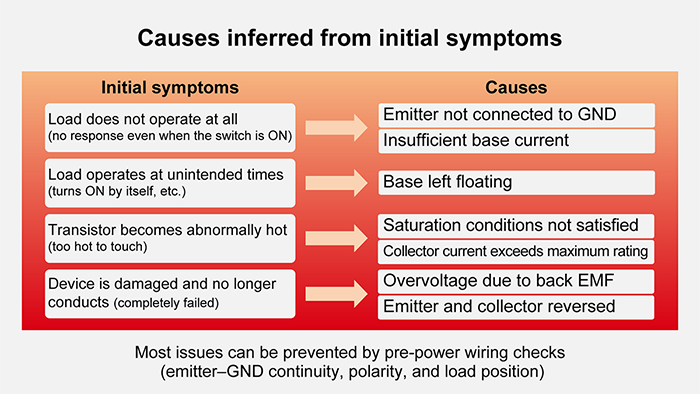
In low-side NPN switches, three problems occur frequently: no operation due to wiring errors, damage from a reverse connection, and overheating from excessive current.
When the load does not operate at all, check whether the emitter is correctly connected to ground and whether the base current is sufficient. When the transistor overheats abnormally, verify that the saturation conditions are satisfied and that the collector current does not exceed the maximum rating.
A few basic wiring checks usually narrow down the cause quickly.
Initial Symptoms of Miswiring, Reverse Connection, and Overcurrent
Problems in low-side wiring can be diagnosed from the observable symptoms. When the load never operates, even with the switch “ON,” either the emitter–ground connection is open, or the base current is insufficient. When the load operates at unintended times, the base is often left floating, allowing noise to drive the transistor into unintended conduction.
When the transistor becomes abnormally hot to the touch, either the saturation conditions are not met—so VCE remains high—or the collector current is exceeding the maximum rating. When the transistor has failed completely and no longer conducts, the most common causes are overvoltage due to back EMF or a reverse connection between the emitter and collector.
Checking the wiring before applying power prevents transistor damage and malfunction. The following three-step procedure is an effective minimum check:
- Verify continuity between the emitter and ground, confirming near-zero resistance with a meter.
- Verify the base resistor connection and load: the collector must connect to the supply through the load, and the emitter must connect to ground.
- Verify the load position: the load must be on the collector side, between the supply and the transistor.
Following this sequence allows most wiring errors to be found before power-on.
Summary
When NPN transistors are used as low-side switches, design success is determined by four elements. The first is the wiring order “Supply → Load → Collector → Emitter → Ground.” If any part of this sequence is reversed, the circuit will not function correctly. The second is meeting the conditions on VBE and VCE(sat). When the base–emitter voltage is about 0.6–0.8 V, the base current is set with a forced β of roughly 10–20, and VCE(sat) falls to around 0.2–0.3 V, the transistor is in saturation. The third is the placement of the flyback diode for inductive loads. Without this protective component, the transistor may be destroyed by back EMF even on the very first switching operation.
Once you understand the correct orientation of the current path, the saturation conditions, the placement of protection circuits, and how to keep the base node from floating, you can reliably drive NPN transistors from microcontroller outputs and reliably switch several hundred milliamperes of load current.
When high-side switching is required, refer to the article on PNP transistor applications. Beyond switching, BJTs are used in analog and electronic circuits as elements in logarithmic converters, temperature sensors, and many other applications.
Related article
Transistor Fundamentals: Structure, Types, and Operating Principles
Bipolar Junction Transistor (BJT) Basics: Operation and Applications (NPN & PNP)
【Download Documents】 Basics of Si Power Devices
In this handbook, although there are so many types of power devices using Si semiconductors, the basic points are explained, focusing mainly on diodes and transistors for power supply applications. It also introduces the procedure and decision method for transistor selection when designing circuits, as well as application examples that utilize each characteristic and feature.

Transistors
Basic
-
Basics of Transistors
- Transistor Fundamentals: Structure, Types, and Operating Principles
- Bipolar Junction Transistor (BJT) Basics: Operation and Applications (NPN & PNP)
- NPN Transistor: Low-Side Switch Fundamentals
- PNP Transistor: High-Side Switch Fundamentals
- MOSFET Basics: Parasitic Capacitance, Gate Charge, Miller Region, and Threshold Voltage
- MOSFET On-Resistance (RDS(on))
- Super junction MOSFET (SJ MOSFET) Basics
- What is a Digital Transistor?
- Digital Transistor Selection
- How to select<Selecting Transistors to Ensure Safe Operation>
- Junction Temperature <Calculating Transistor Chip Temperature>
- What is a Load Switch?
- Basics of MOSFETs
- Introduction
-
Confirming the Suitability of a Transistor in Actual Operation – Introduction
- Confirmation of the Chip Temperature
- Confirmation of Suitability in Actual Operation and Preparations
- Confirmation that Absolute Maximum Ratings are Satisfied
- Confirmation that Operation is within the SOA (Safe Operating Area)
- Confirmation that Operation is within the SOA Derated at the Actual Operating Temperature
- Confirmation that Average Power Consumption is within the Rated Power
- Summary
- Summary
Evaluation
-
The Importance of the Recovery Characteristics of Primary-side Switching Elements in LLC Converters -Introduction-
- Basic Configuration of an LLC Converter
- Features of LLC Converter Operation
- Basic Operation of LLC Converters
- Importance of MOSFET Recovery Characteristics for Off-Resonance of LLC Converters
- The Importance of the Recovery Characteristics of Primary-side Switching Elements in LLC Converters ーSummaryー
-
The Importance of the Reverse Recovery Characteristics of Switching Elements in Inverter Circuits -Introduction-
- Types of Inverter Circuits and Energization Methods
- Basic Operation of 3-Phase Modulation Inverter Circuits
- Comparison of Losses in a PrestoMOS™ MOSFET and a Standard SJ MOSFET Using Double-Pulse Tests (Actual Measurement Results)
- Comparison of Efficiency of a PrestoMOS™ MOSFET and a Standard SJ MOSFET in a 3-Phase Modulation Inverter Circuit (Simulations)
- The Importance of the Reverse Recovery Characteristics of Switching Elements in Inverter Circuits -Summary-
- Mechanisms of MOSFET Destruction
- About Double-Pulse Tests
-
Improving the Power Conversion Efficiency of Phase Shift Full Bridge Circuits – Introduction
- Basic Configuration of a PSFB Circuit
- Basic Operation of PSFB Circuits
- Guidelines Relating to Operation of Switching Elements Under Light Loading
- Guidelines Relating to Operation of Switching Elements Under Heavy Loading
- Evaluation of Efficiency
- Improving the Power Conversion Efficiency of Phase Shift Full Bridge Circuit – Summary –