Transistors|Evaluation
Basic Operation of PSFB Circuits
2021.09.15
Points of this article
・The operation states and current paths, represented as 14 different modes, should be understood.
・Differences in current waveforms occur due to differences in operation. MOSFET losses are different in the leading leg and the lagging leg, and different heat generation results, so that caution must be exercised in thermal design.
・From the equation for the condition for ZVS operation, it is seen that under light loading IL1 is small and so ZVS operation is not readily achieved, but as the load increases, ZVS operation is more easily realized.
ZVS operation in a PSFB circuit is achieved by turning on a MOSFET switch when the output capacitor COSS of the MOSFET is fully discharged and a forward current is flowing through its body diode.
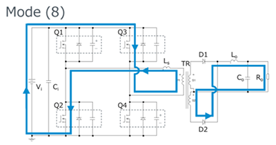
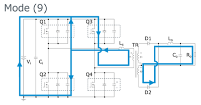
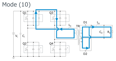
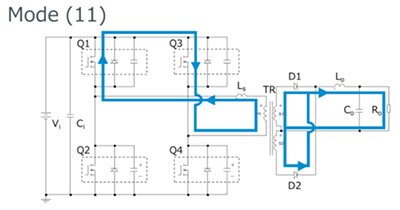
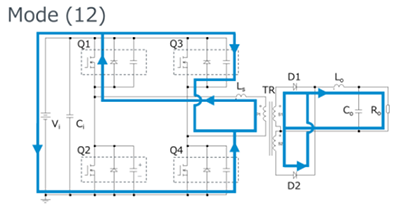
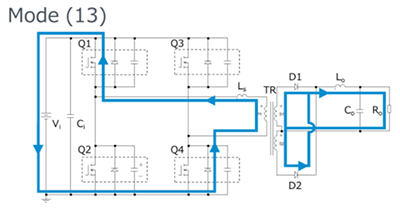
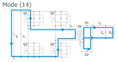
Below are waveforms of the Q1 to Q4 drain currents and the current flowing in the primary-side transformer in a PSFB circuit.
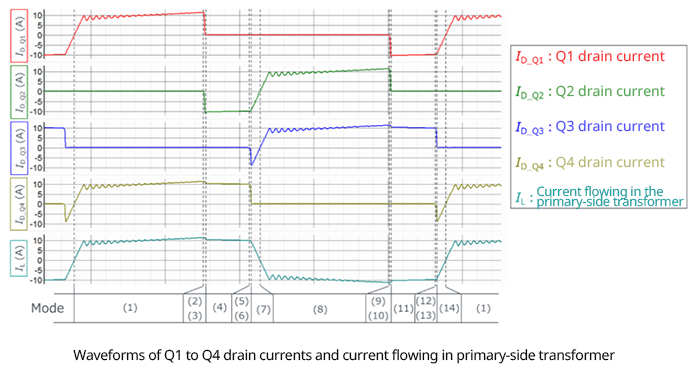
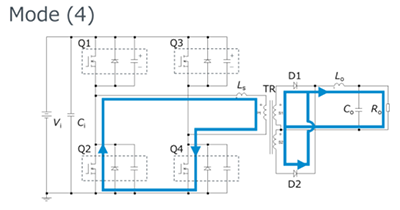
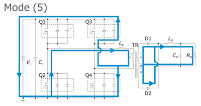
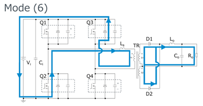
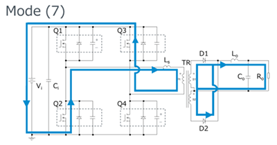
Taking the positive current direction to be the direction from drain to source, we see that for each of Q1 to Q4, there is an interval in which a drain current is flowing in the negative direction, that is, an interval in which a forward current is flowing through the body diode of the MOSFET. For example, in the case of Q3, this is the section of Mode (7). During this interval the drain voltage is nearly zero, and so by turning on the MOSFET during this interval, ZVS operation is achieved.
We also see that it is not the case that the same current waveforms, only shifted in phase, occur in the leading leg and the lagging leg. The reasons for the different waveforms can be understood upon considering the current paths for each of the Modes (1) to (14), indicated below the current waveforms. The numbers and positions of the modes are the same as in the timing chart presented previously.
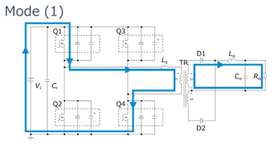
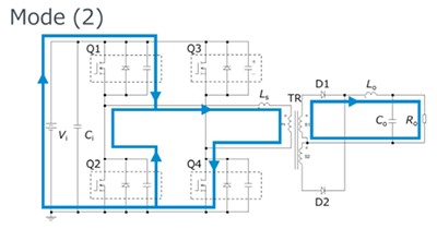
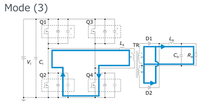
Below, operation and current paths for Modes (1) to (14) are described.
 |
|
 |
|
 |
|
 |
|
 |
|
 |
|
 |
|
 |
|
 |
|
 |
|
 |
|
 |
|
 |
|
 |
|
Due to these changes in current paths, and as explained for Modes (7) and (14) in particular, the turn-on of a MOSFET in the lagging leg causes the input power supply and LS to be series-connected, and the energy in LS decreases rapidly. Because this action does not occur in the leading leg, differences occur in the current waveforms for the leading leg and the lagging leg as a result. Because of these differences in current waveforms, losses are different in the leading-leg MOSFETs and in the lagging-leg MOSFETs, and the amounts of heat generated are different, so care must be exercised in the thermal design.
As in the explanations of Modes (5) and (6) and Modes (12) and (13), in the lagging leg, if the amount of energy stored in LS is not greater than that stored in COSS for a MOSFET, the MOSFET charging and discharging are not completed, and so ZVS operation is not achieved. Hence, if Mode (5) is taken as an example, the condition to achieve ZVS is expressed as equation (1) below. IL1 is IL at the time that Mode (4) ends, and EOSS_Q3 and EOSS_Q4 respectively represent the energy required to complete charging and discharging of the Q3 and Q4 output capacitors.
![]()
From equation (1) we see that under light loading, IL1 is small, so that ZVS operation is not easily achieved, but as the load is increased ZVS operation is more easily realized.
Transistors
Basic
-
Basics of Transistors
- Transistor Fundamentals: Structure, Types, and Operating Principles
- Bipolar Junction Transistor (BJT) Basics: Operation and Applications (NPN & PNP)
- NPN Transistor: Low-Side Switch Fundamentals
- PNP Transistor: High-Side Switch Fundamentals
- MOSFET Basics: Parasitic Capacitance, Gate Charge, Miller Region, and Threshold Voltage
- MOSFET On-Resistance (RDS(on))
- Super junction MOSFET (SJ MOSFET) Basics
- What is a Digital Transistor?
- Digital Transistor Selection
- How to select<Selecting Transistors to Ensure Safe Operation>
- Junction Temperature <Calculating Transistor Chip Temperature>
- What is a Load Switch?
- Basics of MOSFETs
- Introduction
-
Confirming the Suitability of a Transistor in Actual Operation – Introduction
- Confirmation of the Chip Temperature
- Confirmation of Suitability in Actual Operation and Preparations
- Confirmation that Absolute Maximum Ratings are Satisfied
- Confirmation that Operation is within the SOA (Safe Operating Area)
- Confirmation that Operation is within the SOA Derated at the Actual Operating Temperature
- Confirmation that Average Power Consumption is within the Rated Power
- Summary
- Summary
Evaluation
-
The Importance of the Recovery Characteristics of Primary-side Switching Elements in LLC Converters -Introduction-
- Basic Configuration of an LLC Converter
- Features of LLC Converter Operation
- Basic Operation of LLC Converters
- Importance of MOSFET Recovery Characteristics for Off-Resonance of LLC Converters
- The Importance of the Recovery Characteristics of Primary-side Switching Elements in LLC Converters ーSummaryー
-
The Importance of the Reverse Recovery Characteristics of Switching Elements in Inverter Circuits -Introduction-
- Types of Inverter Circuits and Energization Methods
- Basic Operation of 3-Phase Modulation Inverter Circuits
- Comparison of Losses in a PrestoMOS™ MOSFET and a Standard SJ MOSFET Using Double-Pulse Tests (Actual Measurement Results)
- Comparison of Efficiency of a PrestoMOS™ MOSFET and a Standard SJ MOSFET in a 3-Phase Modulation Inverter Circuit (Simulations)
- The Importance of the Reverse Recovery Characteristics of Switching Elements in Inverter Circuits -Summary-
- Mechanisms of MOSFET Destruction
- About Double-Pulse Tests
-
Improving the Power Conversion Efficiency of Phase Shift Full Bridge Circuits – Introduction
- Basic Configuration of a PSFB Circuit
- Basic Operation of PSFB Circuits
- Guidelines Relating to Operation of Switching Elements Under Light Loading
- Guidelines Relating to Operation of Switching Elements Under Heavy Loading
- Evaluation of Efficiency
- Improving the Power Conversion Efficiency of Phase Shift Full Bridge Circuit – Summary –