Transistors|Basic
Bipolar Junction Transistor (BJT) Basics: Operation and Applications (NPN & PNP)
2026.02.17
table of contents
- ・Bipolar Junction Transistor (BJT) Quick Introduction
- ・BJT Structure: Emitter, Base, and Collector Explained
- ・Understanding BJT Operation Through Operating Regions
- ・Basic Connection Methods: Three BJT Configurations and Selection
- ・Minimal BJT Circuits for Practical Learning
- ・Building Amplifier Circuits with BJTs
- ・Key BJT Transistor Parameters to Check in Datasheets
- ・Summary
A bipolar junction transistor (BJT) is a three-terminal semiconductor device that uses a small base current to control a larger collector current. BJTs are widely used for both amplification and switching. Compared with MOSFETs, a BJT requires base current drive, shows stronger temperature dependence, and has a nonzero saturation voltage VCE(sat) when used as a switch. These devices are also called bipolar transistors and are widely used in electronic circuits.
Bipolar Junction Transistor (BJT) Quick Introduction
Bipolar junction transistors (BJTs) serve two primary functions: current amplification and switching. The fundamental difference from MOSFETs lies in whether the device uses current control or voltage control, and this characteristic determines when to use each type. In this article, we focus on BJTs and compare them with MOSFETs (a type of FET) when it helps clarify the design trade-offs.
Organizing Strengths and Weaknesses for Amplification and Switching Applications
BJTs are current-controlled devices, where the base current controls the collector current. In amplification, they can magnify small AC signals by several tens of times, while in switching applications, the required base current depends on the load current. During saturation switching, the effective current gain decreases significantly, so designers choose a base current that satisfies IB ≥ IC/βforced. Here, βforced is the so-called forced current gain, chosen sufficiently below the minimum hFE specified in the datasheet. A common starting point is βforced = 5-10, selected well below the datasheet minimum hFE to provide margin. If base drive is limited, a higher βforced may be unavoidable, so verify VCE(sat) under the actual drive conditions.
Advantages include high current gain and simple circuit configurations. They require few external components and provide stable amplification characteristics from low to mid frequencies.
Key drawbacks are strong temperature dependence and device-to-device variation (especially in hFE). At a roughly constant collector current, the base-emitter voltage, VBE, decreases by about –2 mV/°C with a temperature rise and increases as the collector current increases. The current gain, hFE, can vary by a factor of two, even within the same part number.
BJT Structure: Emitter, Base, and Collector Explained
BJTs consist of three terminals: emitter, base, and collector. Understanding the current relationships between these terminals facilitates the interpretation of circuit diagrams and the identification of operating regions. Physically, a BJT forms two pn junctions in p-type and n-type semiconductor materials: a heavily doped emitter (emitter region) injects majority carriers (e.g., free electrons in an NPN bipolar transistor), a thin, lightly doped base region (small base width) controls flow, and a collector region of moderate doping collects them.
When selecting devices, it is essential to compare BJTs with MOSFETs. MOSFETs are voltage-controlled devices whose drain current is set by the gate voltage, whereas BJTs are current-controlled devices driven by the base current. Therefore, the concepts for driver design and power-loss estimation differ.
What are the Emitter, Base, and Collector? (Understanding Schematic Symbols)
BJTs comprise three terminals called the emitter (E), base (B), and collector (C). In schematic symbols, the arrow attached to the emitter indicates the direction of emitter current (outward for NPN transistor types and inward for PNP transistor types). This arrow direction distinguishes NPN from PNP configurations.
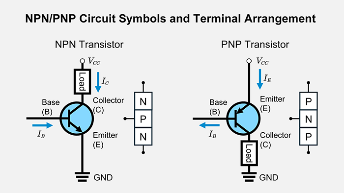
The emitter is heavily doped, the base is a thin layer, and the collector has moderate doping. This three-layer structure enables control of collector current through small base currents. We’ll use conventional current directions and refer explicitly to the emitter terminal, base terminal, and collector when describing schematic symbols and transistor currents (base current IB, collector current IC, and emitter current IE).
NPN vs. PNP Differences (Identifying by Arrow Direction)
In NPN and PNP transistors, the polarities and current directions are inverted. An NPN is commonly used as a low-side switch (it sinks current), with the load connected to VCC. A PNP is commonly used as a high-side switch (it sources current), with the load connected to ground.
An NPN operates as a current sink, while a PNP operates as a current source. These devices are often referred to simply as NPN transistors and PNP transistors, reflecting their opposite current directions.
Understanding BJT Operation Through Operating Regions
BJTs operate in three regions (cutoff, active, and saturation) based on the combinations of applied voltage and current flow. To isolate circuit faults, you need to identify the region in which the transistor is operating based on measured voltages and currents. In the active region, the base–emitter junction is forward-biased (behaving like a diode) while the base–collector junction is reverse-biased. In the cutoff region, both junctions are reverse-biased and only a tiny leakage current flows. In the saturation region, both the base–emitter and base–collector junctions are forward-biased, and the collector–emitter voltage falls low. As a result, the device behaves like a closed switch when used for switching.
Identifying Cutoff, Active Region, and Saturation Region Using VBE, VCE, and IC
| Operating Region | VBE | VCE | |
|---|---|---|---|
| Cutoff | < 0.6 V | ≈ 0 A | ≈ VCC (NPN low-side, load on VCC side) |
| Active | 0.6 to 0.7 V | ≈ β×IB (relationship in active region) | Variable |
| Saturation | 0.7 to 0.9 V | ≈ Load-determined (set by the load and supply) *Condition: IB ≥ IC/βforced |
< 0.3 V |
Table values represent typical values for silicon NPN bipolar transistors and vary depending on the device and current conditions. VBE increases with rising collector current, while VCE(sat) depends on collector current, temperature, and βforced. In the cutoff region, the transistor is off; in the active region, it performs amplification; in the saturation region, it acts as a closed switch. Measure VBE and VCE with a multimeter and calculate IC from the voltage across the load resistor to identify the current operating region. When measured values fall outside these ranges, review the bias circuitry or the load resistance values to ensure they are within acceptable limits. This quick test uses input voltage, measured output voltage, and current flow through the load to classify the region.
Basic Connection Methods: Three BJT Configurations and Selection
The three configurations—common-emitter, common-collector, and common-base—change gain and frequency characteristics depending on which terminal serves as the reference. The common-emitter configuration is designed for amplification, the common-collector configuration focuses on impedance conversion, and the common-base configuration is optimized for high-frequency operation. These three are the standard bipolar transistor configurations.
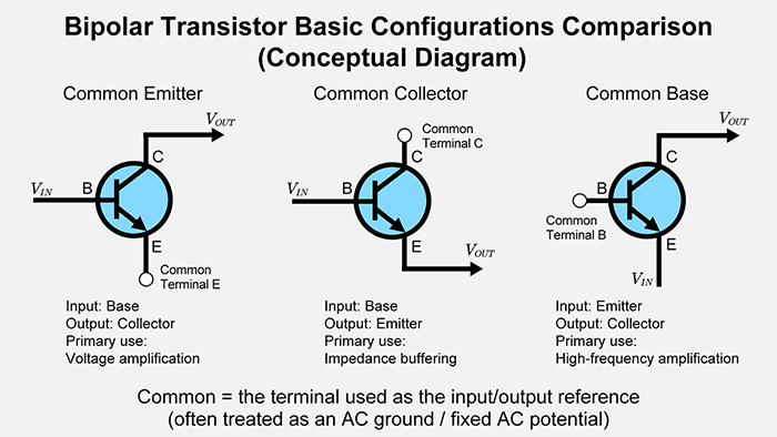
Common Emitter Configuration (CE): High Gain with Phase Inversion
The common-emitter configuration is the most frequently used among BJT configurations. It provides substantial voltage gain with a 180-degree phase inversion. The input impedance is moderate, and the output impedance is relatively high.
Common Collector Configuration (CC): Voltage Gain ≈ 1 (Emitter Follower)
When using BJTs in a common-collector configuration, the voltage gain becomes approximately 1. This common-collector configuration (emitter follower) provides buffering with high input impedance and low output impedance. With its high input impedance and low output impedance, it functions as a buffer between circuit stages. Also called an emitter follower, it transfers signal voltage nearly unchanged while performing impedance conversion.
Common Base Configuration (CB): High-Frequency, Low Current Gain Applications
Its current gain from emitter to collector is close to 1 (slightly less). In many texts this is written as α=IC/IE, where α<1. The common-base configuration of BJTs has a current gain of 1 or less. This common-base configuration is well suited at high frequencies, where BJT operation benefits from low input capacitance. With superior high-frequency characteristics, it’s used in RF amplifiers and mixer circuits. It exhibits low input impedance and high output impedance, making it suitable for wideband amplification requirements.
Minimal BJT Circuits for Practical Learning
In addition to polarity (NPN versus PNP), it is helpful to classify BJTs by use (small-signal, power, RF), configuration (single device or Darlington), and package type (SMD or through-hole). Doing so makes it easier to organize candidate parts and quickly check whether a device can meet the required breakdown voltage, fT, and VCE(sat) targets.
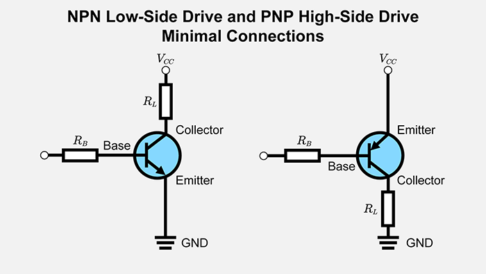
In switching applications, NPN and PNP types require different load connection positions. We’ll examine the differences between low-side drive and high-side drive through practical circuit examples.
NPN Transistor Switching Operation (Low-Side Drive Example)
BJT switching operation can be verified with a minimal circuit configuration. A basic circuit consists of a 5 V supply, an LED with a current-limiting resistor (RL), an NPN transistor, and a base resistor (RB).
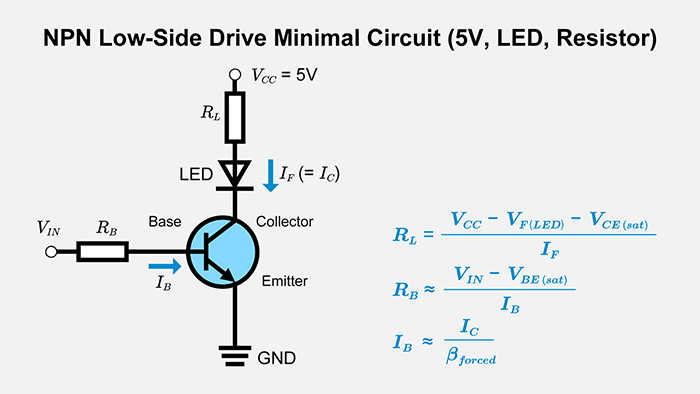
The LED turns on when the control signal goes high and turns off when it goes low. The value of the base resistor RB must account for saturation conditions and base current limiting.
PNP Transistor (High-Side Drive) Differences
PNP transistors turn on when the base is pulled lower than the emitter so that VEB = VE − VB is about 0.6 to 0.8 V. In switching applications, you should also ensure that the reverse base–emitter voltage |VEB| does not exceed the breakdown rating VEBO.
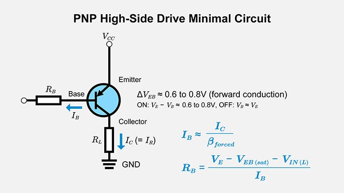
If the control logic cannot drive the base low enough to obtain VEB ≈ 0.6 to 0.8 V for ON, or cannot drive the base close to the emitter (VB ≈ VE) for a reliable OFF state, then a level shifter (e.g., an NPN stage) or a dedicated high-side driver is required.
Building Amplifier Circuits with BJTs
Understanding “Bias Point” First and the IC = β×IB Relationship
In BJT amplifier circuits, setting the bias point (operating point, Q-point) is the initial task. The bias point represents the voltage and current combination at which the transistor operates in the active region, thereby setting the center position so that AC signals can swing positive and negative while remaining within the active region. For small-signal operation, a transistor is characterized by its current gain β, while the stage voltage gain is determined by the load and circuit topology.
The relationship between collector and base currents is often approximated as IC ≈ β × IB, where β (hFE) varies significantly with device, current, temperature, and bias conditions. Because β can vary widely even within the same part number, a bias point designed with a simple β-based calculation can shift: higher-β devices may move toward saturation, while lower-β devices may move toward cutoff. In practical amplifier design, use bias networks and emitter degeneration to reduce β sensitivity, and verify the operating point across the expected β range (e.g., βmin to βmax).
Key BJT Transistor Parameters to Check in Datasheets
Checking hFE(min), VBE, VCE(sat), and fT
In BJT datasheets, verify the maximum ratings and SOA (Safe Operating Area) first. Datasheets plot input characteristics (IB vs. VBE) and output characteristics (IC vs. VCE), which are helpful for circuit analysis and design. After confirming that VCEO, IC, Ptot, Tj, thermal resistance, and SOA curves fall within operating ranges, check hFE(min), VBE, VCE(sat), and fT according to the application. For switching applications, tr, tf, and ts (which are influenced by the stored charge in the device), as well as parasitic capacitances like Cibo and Cobo, are also significant.
hFE(min) is the minimum current gain value used when determining bias circuit resistor values. VBE is the base-emitter voltage needed for base current calculations. VCE(sat) is the collector-emitter voltage at saturation, used when estimating switching circuit losses. fT is the transition frequency, serving as an indicator of the amplifier’s usable frequency bandwidth.
Each parameter varies with temperature and current conditions, requiring verification of the corresponding condition columns in the datasheets.
Summary
Bipolar junction transistors (BJTs) are current-controlled devices in which base current controls collector current. Amplifier circuits operate in the active region, while switching circuits use the cutoff and saturation regions. Operating region identification uses measured values of VBE, VCE, and IC. When the operation differs from expectations, the bias circuitry should be reviewed.
Configuration selection depends on the application. The common-emitter configuration is suitable for amplification requiring high gain, the common collector targets impedance conversion, and the common-base works well for high-frequency operation. NPN typically serves in low-side drive while PNP serves in high-side drive, each with opposite current directions and control reference potentials.
In datasheets, first verify maximum ratings and SOA, then check hFE(min), VBE, VCE(sat), and fT according to the application. Design with minimum hFE values, taking into account temperature and current conditions.
Related article
Transistor Fundamentals: Structure, Types, and Operating Principles
【Download Documents】 Basics of Si Power Devices
In this handbook, although there are so many types of power devices using Si semiconductors, the basic points are explained, focusing mainly on diodes and transistors for power supply applications. It also introduces the procedure and decision method for transistor selection when designing circuits, as well as application examples that utilize each characteristic and feature.

Transistors
Basic
-
Basics of Transistors
- Transistor Fundamentals: Structure, Types, and Operating Principles
- Bipolar Junction Transistor (BJT) Basics: Operation and Applications (NPN & PNP)
- NPN Transistor: Low-Side Switch Fundamentals
- PNP Transistor: High-Side Switch Fundamentals
- MOSFET Basics: Parasitic Capacitance, Gate Charge, Miller Region, and Threshold Voltage
- MOSFET On-Resistance (RDS(on))
- Super junction MOSFET (SJ MOSFET) Basics
- What is a Digital Transistor?
- Digital Transistor Selection
- How to select<Selecting Transistors to Ensure Safe Operation>
- Junction Temperature <Calculating Transistor Chip Temperature>
- What is a Load Switch?
- Basics of MOSFETs
- Introduction
-
Confirming the Suitability of a Transistor in Actual Operation – Introduction
- Confirmation of the Chip Temperature
- Confirmation of Suitability in Actual Operation and Preparations
- Confirmation that Absolute Maximum Ratings are Satisfied
- Confirmation that Operation is within the SOA (Safe Operating Area)
- Confirmation that Operation is within the SOA Derated at the Actual Operating Temperature
- Confirmation that Average Power Consumption is within the Rated Power
- Summary
- Summary
Evaluation
-
The Importance of the Recovery Characteristics of Primary-side Switching Elements in LLC Converters -Introduction-
- Basic Configuration of an LLC Converter
- Features of LLC Converter Operation
- Basic Operation of LLC Converters
- Importance of MOSFET Recovery Characteristics for Off-Resonance of LLC Converters
- The Importance of the Recovery Characteristics of Primary-side Switching Elements in LLC Converters ーSummaryー
-
The Importance of the Reverse Recovery Characteristics of Switching Elements in Inverter Circuits -Introduction-
- Types of Inverter Circuits and Energization Methods
- Basic Operation of 3-Phase Modulation Inverter Circuits
- Comparison of Losses in a PrestoMOS™ MOSFET and a Standard SJ MOSFET Using Double-Pulse Tests (Actual Measurement Results)
- Comparison of Efficiency of a PrestoMOS™ MOSFET and a Standard SJ MOSFET in a 3-Phase Modulation Inverter Circuit (Simulations)
- The Importance of the Reverse Recovery Characteristics of Switching Elements in Inverter Circuits -Summary-
- Mechanisms of MOSFET Destruction
- About Double-Pulse Tests
-
Improving the Power Conversion Efficiency of Phase Shift Full Bridge Circuits – Introduction
- Basic Configuration of a PSFB Circuit
- Basic Operation of PSFB Circuits
- Guidelines Relating to Operation of Switching Elements Under Light Loading
- Guidelines Relating to Operation of Switching Elements Under Heavy Loading
- Evaluation of Efficiency
- Improving the Power Conversion Efficiency of Phase Shift Full Bridge Circuit – Summary –