Transistors|Basic
Transistor Fundamentals: Structure, Types, and Operating Principles
2026.02.06
table of contents
- ・Understanding the Basics and Functions of Transistors
- ・Basic Structure and Operating Principles of Transistors
- ・Main Transistor Types and Characteristics
- ・Confirming Transistor Operation in Simple Circuits
- ・Key Parameters in Transistor Circuit Design
- ・Main Transistor Applications and Examples
- ・Summary: Transistor Fundamentals and Next Steps
A transistor is a semiconductor device that amplifies weak signals and switches current on or off. You’ll find transistors doing both jobs in analog and digital circuits. Smartphone processors pack billions of transistors. Audio amplifiers use them to boost microphone signals to levels that can drive speakers. These electronic devices are ubiquitous in modern electronics, replacing vacuum tubes that dominated earlier generations. This article explains how transistors work, their primary types, and their role in circuits.
Understanding the Basics and Functions of Transistors
What transistors do becomes clearer when you separate the device itself from its role in a circuit. Understanding what a transistor is at the component level helps you see how it fits into larger electronic circuits.
What Is a Transistor? Amplification and Switching with Semiconductor Materials
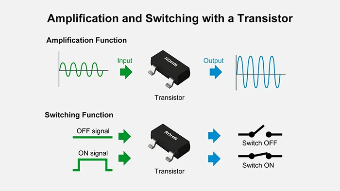
Transistors convert small input signals into large output signals. This behavior comes from doped semiconductors (such as silicon), where p-type and n-type regions let current flow be controlled. These impurities create regions where the flow of electrical current can be controlled. Small voltage or current changes at the input can result in significantly larger changes at the output. The transistor acts as either an amplifier or a switch, depending on the circuit’s configuration.
In amplification mode, electronic signals at the input get boosted anywhere from a few times to a few hundred times. Audio amplifiers take the weak microphone signal and amplify it enough to drive speakers. The transistor pulls energy from the power supply and adds it to the output. The original waveform remains intact as its amplitude increases. Within its linear region, the amplifier preserves the waveform while increasing its amplitude.
Switching works differently. The transistor rapidly switches between conducting (on) and blocking (off) states. Digital logic circuits use these two states as logic 0 and 1. This is the basis of digital computation and memory. A CPU has billions of transistors switching in nanoseconds to handle complex processing.
Whether a transistor acts as an amplifier or a switch depends on its biasing (operating region). Amplification requires an active region, where the output remains proportional to the input. Switching runs the transistor fully on (in saturation) or entirely off (in cutoff). Changing the circuit design results in the same transistor performing completely different functions. That versatility is what makes transistors powerful.
The Role Transistors Play in Electronic Circuits
Analog circuits use transistors to amplify weak signals from sensors. A temperature sensor might output a few millivolts. A microcontroller’s ADC input typically expects a signal within its input/reference range (for example, 0–3.3 V), so transistor amplifiers (or op-amps) are used to scale small sensor outputs. Transistor amplifiers handle this conversion while maintaining the signal’s accuracy and fidelity. Add a filter circuit, and you can pull out specific frequencies while attenuating noise.
Digital circuits are constructed from logic gates built with transistors. These gates are the basic building blocks of computation. AND, OR, NOT operations all come from combining multiple transistors. By building up layers of these gates, you get adders, comparators, and memory cells. Integrated circuits, such as microcontrollers and FPGAs, contain countless transistors that run in sync with a clock signal, executing the instructions provided by the program.
Power circuits use transistors for voltage and current regulation. Switching supplies use high-frequency on/off cycles to convert one voltage to another. Linear regulators enable transistors to act like adjustable resistors, maintaining a steady output voltage as the load changes. LED drivers and motor controllers use transistors to regulate current flow and deliver the required power.
Interface circuits use transistors to bridge different voltage levels. Connecting a 3.3V microcontroller to a 5V sensor? A transistor-based level shifter handles the translation. This lets you mix parts from different generations without compatibility issues.
Basic Structure and Operating Principles of Transistors
Transistors have three terminals. Each one does something specific when controlling current. If you understand how the PN junctions between these terminals work, you’ll appreciate signal amplification and current control.
Roles of the Three Terminals: Emitter, Base, and Collector
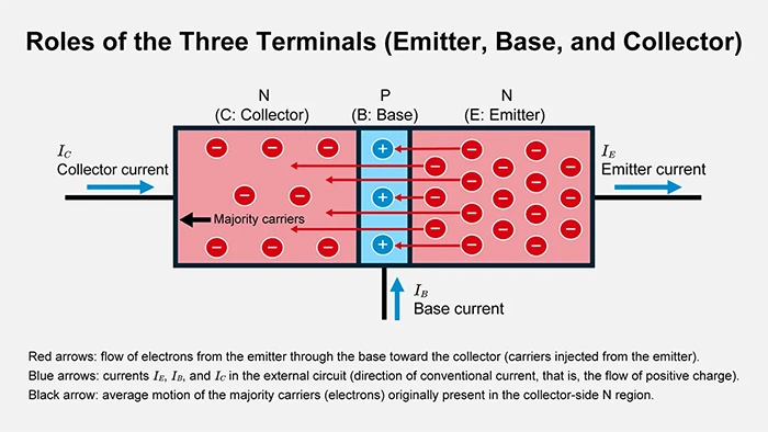
A bipolar junction transistor has three terminals: emitter, base, and collector. In an NPN BJT operating in the active region, electrons flow from the emitter to the collector, while conventional current in the external circuit flows from the collector to the emitter. A small base current controls a much larger collector current. In an NPN transistor, applying a positive voltage to the base makes base current flow. This triggers collector current. The collector current ends up tens to hundreds of times larger than the base current. That ratio is the current gain. PNP transistors flip the carrier types, but the control works the same way.
When the base-emitter voltage reaches approximately 0.6 to 0.7V for silicon, carriers begin to move from the emitter into the base. The emitter base junction controls this carrier injection. Most of these carriers pass through the base region and reach the collector. What doesn’t make it to the collector flows out as base current. The emitter current is split between the collector current and the base current. Thinner base? More carriers reach the collector—resulting in higher current gain.
The power supply voltage connects to the collector-emitter, creating a path for the collector current. There is enough voltage, and the collector current tracks the base current proportionally. Active mode works this way. Drop the collector-emitter voltage too low, and you hit saturation. Adding more base current does nothing to increase the collector current at that point. Switching uses saturation for “on” and cutoff for “off”.
PN Junction Basics: Forward and Reverse Bias
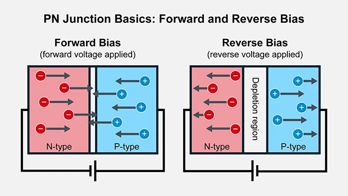
A PN junction joins P-type and N-type semiconductor materials. P regions have lots of holes. N regions have lots of electrons. At the junction, electrons and holes diffuse across and recombine with each other. This creates a depletion region with no carriers. The depletion region blocks current flow.
Forward bias applies a positive voltage to the P side and a negative voltage to the N side. The depletion region shrinks. Carriers can now cross the junction more easily. Holes move from P to N, electrons from N to P. Current flows. Once the voltage passes the threshold (about 0.6 to 0.7V for silicon), the current jumps sharply.
Reverse bias flips it. Negative on P, positive on N. The depletion region expands. Carrier movement stops. The majority carrier current stops. All you see is a small leakage from minority carriers. If you increase the reverse voltage too far, electrons in the depletion region acquire enough energy to initiate an avalanche effect. If the reverse voltage exceeds the rating, the junction enters breakdown; without current limiting, this can overheat and damage the device.
In active mode, the base–emitter junction is forward-biased and the base–collector junction is reverse-biased, so carriers injected from the emitter are swept into the collector by the electric field. This allows a small base current to control a much larger collector current.
Main Transistor Types and Characteristics
Transistors are categorized into two primary types: current-controlled bipolar transistors and voltage-controlled field-effect transistors. They work differently. Understanding these transistor types and selecting the appropriate one is crucial for achieving design efficiency and optimal performance.
Bipolar Junction Transistors (BJT): NPN and PNP
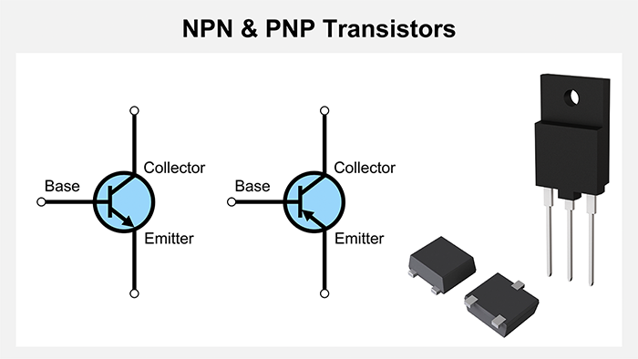
Bipolar junction transistors (BJT) use both electrons and holes to carry current. Two types exist: the NPN transistor and the PNP transistor. They differ in how the semiconductor layers are stacked. NPN stacks N-P-N, PNP stacks P-N-P. Most circuits use NPN transistors because electrons move faster than holes, which makes NPN devices better suited for high-speed operation.
NPN transistors conduct when a positive voltage is applied to the base. Electrons move from emitter to collector. The power supply’s positive terminal is connected to the collector, and the negative terminal is connected to the emitter. Small positive current through the base drives the collector current. Typical small-signal transistors handle collector currents from a few milliamps to hundreds of milliamps with base currents in the microamp to milliamp range.
PNP transistors reverse the polarities and current directions. A negative base voltage causes holes to flow from the emitter to the collector. Mixing NPN and PNP transistors enables the construction of push-pull or complementary circuits, which are beneficial for efficient power amplification and bidirectional switching.
The input impedance ranges from several kilohms to tens of kilohms. You need to supply the base current. Current gain varies with temperature and operating point; therefore, circuits employ negative feedback and bias to stabilize their operation. High gain and low noise make them popular for amplifying weak signals in analog work.

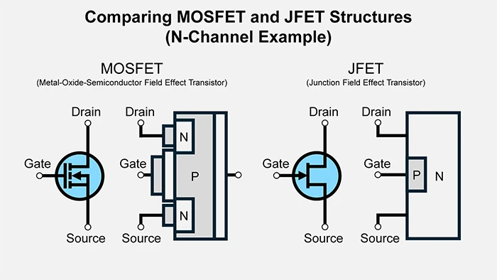
Field-Effect Transistors(FETs) : MOSFETs and JFETs
Field-effect transistors control current with voltage and have three terminals: gate, source, and drain. Gate voltage controls source-drain current. Almost no gate current flows, unlike bipolar types. High input impedance means less load on the drive circuit. The electric field from the gate voltage modulates the channel conductivity.
MOSFETs have a metal-oxide-semiconductor structure. An oxide layer sits between the gate electrode and the semiconductor. Gate voltage forms a channel at the semiconductor surface. There are two main types: N-channel and P-channel devices. The N-channel turns on with a positive gate voltage, while the P-channel turns on with a negative gate voltage. Digital circuits often use CMOS, which combines n-type and p-type transistors. In CMOS, static power is very low (ideally only leakage). Most power is consumed during switching due to charging/discharging capacitances and brief short-circuit current during transitions.
JFETs use PN junctions to form channels. Reverse-biasing the gate widens the depletion region, thereby restricting the source-drain current. They have a simpler structure than MOSFETs and often offer better noise performance. They are common in RF circuits and analog front-ends. JFETs typically operate in depletion mode. Current flows with zero gate voltage.
The gate current is negligible, allowing sensor circuits and buffers to operate without loading the signal source. MOSFETs excel at fast switching and low on-resistance for power and motor control. JFETs excel in low-noise applications, such as audio and instrumentation.
Note: Vth indicates when conduction begins. For actual drive capability, check VGS where RDS(on) is specified (like 4.5V or 10V) and calculate the loss with your required current.
Selecting Transistors for Your Application
Start with circuit requirements. Amplifiers require bandwidth, gain, and noise specifications. Switching circuits are concerned with on-resistance, speed, and voltage rating. Power circuits consider dissipation, thermal resistance, and the type of package. Discrete transistors give you flexibility in matching specific circuit needs.
Bipolar junction transistors are well-suited for low to mid-frequency amplification or when high current drive is required. High current gain means a tiny base current controls a big collector current, which makes BJTs a good choice for sensor amplification and analog computation.
MOSFETs are capable of handling fast switching and high currents. Vth tells you when conduction starts. For actual drive capability, check VGS where RDS(on) is specified (like 4.5V or 10V) and calculate the loss with your required current. Switching supplies benefit from low on-resistance, resulting in less conduction loss and higher efficiency.
Refer to the datasheet for maximum ratings and recommended operating conditions. Look at the collector or drain dissipation based on actual power and your thermal design. At high ambient temperatures, you must derate the specifications.
Confirming Transistor Operation in Simple Circuits
Theory only goes so far. Actual circuits make transistor behavior concrete. Two standard configurations show how voltage and current relate at the terminals.
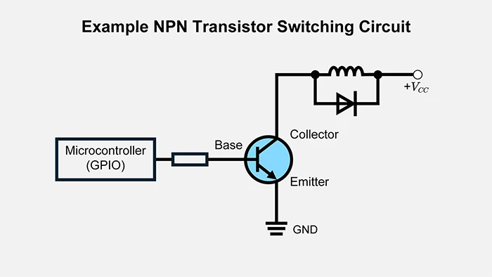
Basic Switching Circuit (NPN Transistor)
NPN switching circuits are standard for microcontroller control of LEDs, relays, and similar loads. The power supply is connected to the load, the load is connected to the collector, and the emitter is connected to ground. The microcontroller output feeds the base through a resistor. This turns the load current on and off.
The base resistor needs to pass enough current to saturate the transistor. In saturation, the collector-emitter voltage drops to tens or hundreds of millivolts. Transistor loss stays minimal. Base-resistor design details are covered in more detailed design articles.
Inductive loads generate back EMF when the transistor is turned off. Too much voltage causes a breakdown. Solution: a freewheeling diode across the load. Cathode to the power side, anode to the collector side. The diode absorbs the back EMF current, protecting the transistor.
When the microcontroller output is high, the transistor turns on, allowing current to flow through the load. When the output is low, the transistor turns off and the current stops. This provides a simple and effective way to control power using digital signals.
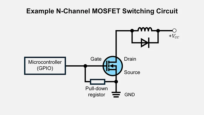
Basic Switching Circuit (N-ch MOSFET)
N-channel MOSFETs are well-suited for high-current loads and fast-switching applications. Connect the power supply to the load, the load to the drain, and the source to ground. The microcontroller output drives the gate and controls the load current.
The gate-source voltage controls the MOSFET, and since almost no gate current flows, microcontrollers can sometimes drive gates directly. Gate drive details are in the lower-level design articles.
A floating gate can cause unintended turn-on due to static charge or stray electric fields. Static electricity or stray fields can activate the device when you don’t want it to. A pull-down resistor between gate and source fixes this by keeping the gate voltage at zero when the microcontroller isn’t driving it.
Inductive loads require freewheeling diodes, just as with NPN transistors. Connect the diode across the load to absorb back EMF current. Low on-resistance reduces conduction loss. Switching loss depends on transition time, gate charge, switching frequency, and the voltage/current overlap during switching.
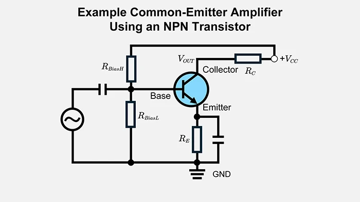
Basic Amplifier Circuit with Transistors (Common Emitter)
The common emitter is the standard bipolar amplifier topology. The emitter is the reference node. The input signal goes to the base. The amplified signal comes from the collector. The collector resistor connects the collector to the power supply, and the emitter resistor connects the emitter to ground. The base gets a voltage divider bias circuit.
Bias sets the transistor at a proper DC operating point with no input signal. Place this point near the mid-supply point to maximize the range for clean amplification in both directions. The emitter resistor provides DC negative feedback and stabilizes the bias point. A bypass capacitor placed in parallel with the emitter resistor increases AC gain by reducing emitter degeneration at signal frequencies. When emitter current increases, the voltage drop across the emitter resistor rises, effectively reducing the base-emitter voltage. This action automatically adjusts the collector current and stabilizes the operating point. When the base current changes at the input, the collector current follows. The voltage drop across the collector resistor changes, causing the output to invert from the input. That phase inversion, combined with high voltage gain, defines common emitter operation.
Key Parameters in Transistor Circuit Design
Circuit design involves accurately reading datasheet specifications and estimating operating conditions. If you account for input/output characteristics and thermal design basics correctly, your circuit will operate reliably.
Input Characteristics: Base-Emitter Voltage, Threshold Voltage, Input Impedance
The base–emitter voltage, VBE, indicates when a silicon BJT begins to conduct. At room temperature, VBE is typically about 0.6–0.7 V at moderate current levels. At approximately constant collector current, VBE decreases by about 2 mV/°C as temperature rises. Bias networks should be designed so the operating point remains stable across temperature and device variation.
The MOSFET threshold voltage, VGS(th), is specified at a very small drain current and indicates only the onset of conduction—it is not the gate voltage required for low-loss switching. For switching applications, choose a MOSFET with RDS(on) specified at your available gate-drive voltage (commonly 4.5 V or 10 V), and verify worst-case performance over temperature and tolerances.
The input impedance is what the signal source sees when looking into the transistor. Bipolar types pass base current, so the input impedance sits at several kilohms to tens of kilohms. High source impedance means the base current can pull down the signal voltage. Gain deviates from design values.
MOSFETs have essentially infinite DC input impedance because the gate oxide acts as an insulator. However, there is gate-source capacitance. At high frequencies or during rapid switching, charging this capacitance is crucial. AC impedance drops. Fast switching with large gate capacitance requires a low-impedance drive circuit.
Output Characteristics: Collector Current, Output Voltage, Voltage Drop
Collector current, IC, is the main controlled output in a BJT. Datasheets specify a maximum continuous collector current, but the usable current in a design is typically limited by power dissipation, package thermal resistance, and the device’s safe operating area (SOA). In practice, keep adequate margin below absolute maximum ratings and verify worst-case conditions (temperature, cooling, tolerances, and SOA). Pulsed currents may exceed the DC rating if they remain within the SOA and the average power dissipation stays within limits.
The collector-emitter voltage indicates the drop in saturation. Saturation brings it down to tens or hundreds of millivolts. Switching in saturation minimizes transistor loss. Operating in active mode varies the collector-emitter voltage from a few volts up to near the supply voltage. Amplification works in this range.
MOSFET on-resistance is the drain-source resistance when the device is conducting. It typically ranges from milliohms to hundreds of milliohms. Lower is better for conduction loss. On-resistance increases with temperature, so continuous operation needs loss calculations at elevated temperatures. High-current circuits make on-resistance the primary source of heat.
The output voltage range depends on the load resistance and the transistor state. Bigger collector resistance means bigger voltage swing, but limited current. Switching circuits require a small on-state drop and a full supply voltage when off. Amplifiers adjust the operating point and collector resistance so that the output doesn’t reach saturation or cutoff with the input signal amplitude.
Power Consumption and Thermal Design: Heat and Temperature Management
Transistor power dissipation is primarily the sum of conduction loss and switching loss. For a BJT, a first-order estimate of conduction loss is Pcond ≈ VCE × IC (use average values for the operating condition; in saturation use VCE(sat)). For a MOSFET, conduction loss is Pcond ≈ ID(RMS)2 × RDS(on) (use the RDS(on) value at the operating junction temperature). Switching loss occurs during transitions when voltage and current overlap; you can estimate it from transition times (and switching frequency) or use switching-energy values from the datasheet.
Maximum allowable power dissipation is limited by the junction temperature rating, Tj,max. Datasheets provide a power-derating curve versus case or ambient temperature; above a reference temperature (often 25°C), PD(max) typically decreases approximately linearly according to the relevant thermal resistance ( θJA or θJC, depending on the mounting condition).
Thermal resistance (θ, in °C/W) quantifies how difficult it is for heat to flow out of the device. When heat flows through several layers, the thermal resistances add in series, and the temperature rise is ΔT ≈ P × θtotal. For a heatsinked package, θtotal ≈ θJC + θCS + θSA. For surface-mount devices, the effective θJA strongly depends on PCB copper area and vias, so board layout becomes part of the thermal design.
In formula form, the junction temperature can be estimated as Tj ≈ Ta + P × (θJC + θCS + θSA) when using a heatsink (all θ in °C/W and P in W). If no heatsink is used and the datasheet provides θJA for the intended PCB condition, a simpler estimate is Tj ≈ Ta + P × θJA. For reliability, design with a comfortable margin below Tj,max (for example, target Tj at least 20–30°C below Tj,max, depending on lifetime and environment).
Thermal design takes into account the package type and mounting method. Large packages, such as TO-220 or TO-247, can be mounted on heatsinks. Suitable for high power. Surface-mount packages use board thermal vias and copper pours as thermal paths. For continuous operation, calculate worst-case junction temperature (maximum ambient, worst-case power dissipation, and worst-case thermal resistance) to ensure adequate margin against overheating. Choose a junction-temperature target that meets the required reliability, rather than operating close to Tj,max.
Main Transistor Applications and Examples
Transistors do different things in digital circuits, analog circuits, and power electronics. Understanding these differences helps with selecting the appropriate components.
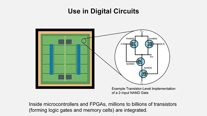
Transistors in Digital Circuits: Switching and Logic Gates
Digital circuits switch transistors between on and off to perform logic and process information. CMOS pairs N-channel and P-channel MOSFETs so that when one is on, the other is off. This arrangement forms logic gates. Combine inverters to create NAND, NOR, and XOR gates. Microcontrollers and FPGAs contain from millions to billions of transistors, enabling complex operations to run in parallel.
Transistors in Analog Circuits: Amplifying Weak Signals
Sensor circuits use transistors to amplify weak signals before sending them downstream. Temperature sensors and strain gauges output a few millivolts to tens of millivolts. Microcontroller ADCs need a higher voltage. Audio amplifiers provide voltage gains ranging from hundreds to thousands in the preamp stage, followed by current amplification in the power stage to match the speaker impedance. Differential amplifiers pair transistors to cancel temperature and supply voltage effects while detecting and amplifying minor voltage differences.
Transistors in Power Electronics
Switching supplies cycle transistors on and off at high frequency for voltage conversion. The low on-resistance and fast switching of MOSFETs can yield efficiencies over 90%. Motor drivers use PWM to control average current and regulate speed. LED drivers combine transistors with sense resistors for constant current and stable light output. Inverters convert DC to AC for solar systems and backup power. High-voltage applications often use insulated-gate bipolar transistors (IGBTs), which combine MOSFET-like drive characteristics with BJT-like current-handling capability. Power transistors in these applications push the limits on voltage and current ratings while maintaining efficiency.
Summary: Transistor Fundamentals and Next Steps
This article covered transistor mechanisms, types, and roles across electronic circuits. Bipolar junction transistors use current control, MOSFETs use voltage control. Understanding these principles and knowing how to select the right electronic devices for your application gives you the foundation for practical design work.
【Download Documents】 Silicon Power Devices Application Examples Utilizing the Merits
ROHM's seminar materials provided at the seminar venue. Silicon base power devices continue its evolution for the market demands of product power saving and efficiency enhancing. Basic knowledge to selection methods for diodes and MOSFETs, the latest device properties, and application examples are described.

Transistors
Basic
-
Basics of Transistors
- Transistor Fundamentals: Structure, Types, and Operating Principles
- Bipolar Junction Transistor (BJT) Basics: Operation and Applications (NPN & PNP)
- NPN Transistor: Low-Side Switch Fundamentals
- PNP Transistor: High-Side Switch Fundamentals
- MOSFET Basics: Parasitic Capacitance, Gate Charge, Miller Region, and Threshold Voltage
- MOSFET On-Resistance (RDS(on))
- Super junction MOSFET (SJ MOSFET) Basics
- What is a Digital Transistor?
- Digital Transistor Selection
- How to select<Selecting Transistors to Ensure Safe Operation>
- Junction Temperature <Calculating Transistor Chip Temperature>
- What is a Load Switch?
- Basics of MOSFETs
- Introduction
-
Confirming the Suitability of a Transistor in Actual Operation – Introduction
- Confirmation of the Chip Temperature
- Confirmation of Suitability in Actual Operation and Preparations
- Confirmation that Absolute Maximum Ratings are Satisfied
- Confirmation that Operation is within the SOA (Safe Operating Area)
- Confirmation that Operation is within the SOA Derated at the Actual Operating Temperature
- Confirmation that Average Power Consumption is within the Rated Power
- Summary
- Summary
Evaluation
-
The Importance of the Recovery Characteristics of Primary-side Switching Elements in LLC Converters -Introduction-
- Basic Configuration of an LLC Converter
- Features of LLC Converter Operation
- Basic Operation of LLC Converters
- Importance of MOSFET Recovery Characteristics for Off-Resonance of LLC Converters
- The Importance of the Recovery Characteristics of Primary-side Switching Elements in LLC Converters ーSummaryー
-
The Importance of the Reverse Recovery Characteristics of Switching Elements in Inverter Circuits -Introduction-
- Types of Inverter Circuits and Energization Methods
- Basic Operation of 3-Phase Modulation Inverter Circuits
- Comparison of Losses in a PrestoMOS™ MOSFET and a Standard SJ MOSFET Using Double-Pulse Tests (Actual Measurement Results)
- Comparison of Efficiency of a PrestoMOS™ MOSFET and a Standard SJ MOSFET in a 3-Phase Modulation Inverter Circuit (Simulations)
- The Importance of the Reverse Recovery Characteristics of Switching Elements in Inverter Circuits -Summary-
- Mechanisms of MOSFET Destruction
- About Double-Pulse Tests
-
Improving the Power Conversion Efficiency of Phase Shift Full Bridge Circuits – Introduction
- Basic Configuration of a PSFB Circuit
- Basic Operation of PSFB Circuits
- Guidelines Relating to Operation of Switching Elements Under Light Loading
- Guidelines Relating to Operation of Switching Elements Under Heavy Loading
- Evaluation of Efficiency
- Improving the Power Conversion Efficiency of Phase Shift Full Bridge Circuit – Summary –