Transistors|Basic
MOSFET Basics: Parasitic Capacitance, Gate Charge, Miller Region, and Threshold Voltage
2026.06.04
A metal‑oxide‑semiconductor field‑effect transistor (MOSFET) is a voltage‑driven semiconductor switch that can control large drain currents with gate‑to‑source voltage (VGS). Unlike a bipolar junction transistor (BJT), a MOSFET does not require continuous drive current in steady state; instead, switching is dominated by charging and discharging the gate’s parasitic capacitances. As a result, gate charge and parasitic capacitances largely determine switching speed, switching loss, and dV/dt‑related behavior.
In practical switching designs (switch‑mode power supplies, load switches, and half‑bridges), four datasheet parameters are especially important: input capacitance (Ciss), reverse transfer capacitance (Crss), total gate charge (Qg), and gate threshold voltage (VGS(th)). This article explains how to interpret these parameters and how they map to switching time, loss, and inadvertent turn‑on risk.”
The overall picture of transistors and the operating principles of BJTs are covered in “Transistor Fundamentals” and “Bipolar Junction Transistor (BJT) Basics”, so this section focuses only on explaining parameters specific to MOSFETs.
MOSFET Structure and Gate Control
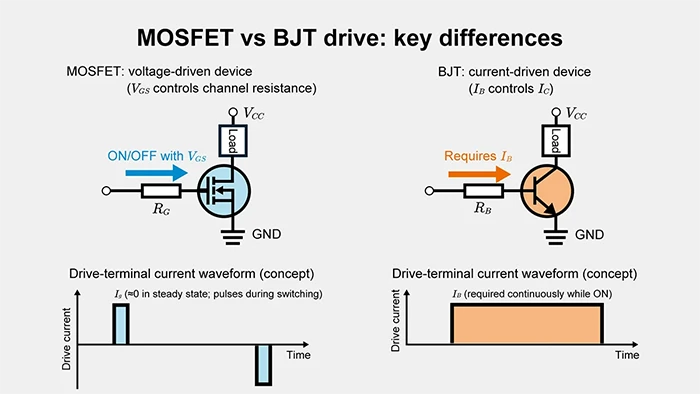
MOSFETs control large currents with gate voltage alone. Applying a positive gate-to-source voltage (VGS) creates a conducting channel in the semiconductor, letting current flow between the source and drain terminals. BJTs operate by flowing base current; In steady state, the MOSFET gate draws essentially no DC (aside from leakage). However, during switching, the driver must source and sink current to move charge into and out of the gate capacitances, and this transient gate current largely determines switching speed and loss.
MOS Structure and N-Channel (Nch) / P-Channel (Pch) Differences
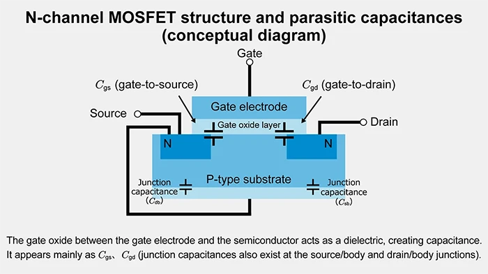
An n-channel MOSFET forms N-type source and drain regions on a P-type semiconductor substrate. Positive gate voltage creates an electron channel just below the gate oxide layer. A p-channel MOSFET has P-type source and drain on an N-type substrate, forming a hole channel with a negative gate-to-source voltage (VGS<0). N-channel devices offer higher speed due to superior electron mobility; P-channel devices can simplify driver circuits in high-side switches. The channel width affects both on-resistance and parasitic capacitance. Wider channels lower resistance but increase capacitance.
A very thin layer of silicon dioxide separates the gate electrode from the semiconductor surface. This thin insulating layer acts as the gate oxide dielectric and forms the MOS capacitor structure. Source and drain junctions add depletion-region capacitance. These combine to appear as parasitic capacitances in the datasheet. N-channel and P-channel differ in absolute values, but the correspondence and how you handle them in switching design are the same.
Differences from BJTs and the Benefit of High Input Impedance
BJTs are current-driven devices. Base current controls collector current, with operating point set by base–emitter forward drop (approximately 0.7 V) and current gain hFE. Power MOSFETs are voltage-driven devices. Applied gate voltage modulates channel conductivity, and the steady-state gate current remains near leakage levels. High driver output resistance produces minimal steady-state power loss.
Switching transients force charge in and out of the gate capacitance through the gate bias circuit, loading the gate driver IC. Large parasitic capacitance lengthens charge/discharge times, raising switching loss and dV/dt-induced noise. High input impedance helps steady operation, but the capacitive load during transients is a key design consideration unique to MOSFET switching behavior.
Key Switching Parameters
Datasheets list on-resistance, parasitic capacitance, total gate charge, gate threshold voltage, maximum drain current, and breakdown voltage. On-resistance sets conduction loss; maximum current and breakdown voltage set the device’s absolute maximum ratings (current/voltage). This article focuses on parameters that directly affect switching speed and switching loss.
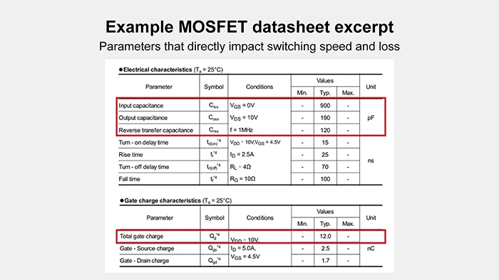
Input capacitance (Ciss) loads the gate driver. Reverse transfer capacitance (Crss, feedback capacitance) creates Miller effect delay. Output capacitance (Coss) exchanges charge when drain voltage swings. Total gate charge (Qg) is the charge required to turn on the gate fully and is used for switching loss estimates. The gate threshold voltage marks the onset of channel formation and is used to set margin against inadvertent turn-on.
Parasitic Capacitance in MOSFETs
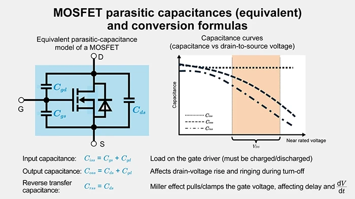
MOSFET parasitic capacitance appears in datasheets as three values: input capacitance (Ciss), output capacitance (Coss), and reverse transfer capacitance (Crss). These combine gate–source, gate–drain, and drain–source capacitances. Input capacitance is what the gate driver must charge. Reverse transfer capacitance causes Miller delay. Output capacitance exchanges charge during drain voltage swings.
Capacitance Components and Datasheet Notation
Gate–source capacitance (Cgs) is the oxide-layer capacitance between the gate electrode and the source terminal and remains nearly constant. Gate–drain capacitance (Cgd) shrinks as drain voltage rises because the depletion region widens, effectively increasing the “plate separation” in the capacitive structure. Drain–source capacitance (Cds) also depends on drain voltage.
Datasheet capacitance parameters are defined as follows.
Input capacitance, measured with drain shorted to source:
\(C_{iss}=C_{gs}+C_{gd}\)
Output capacitance, measured across drain and source with gate shorted to source:
\(C_{oss}=C_{ds}+C_{gd}\)
Reverse transfer capacitance, which corresponds to the gate–drain capacitance:
\(C_{rss}=C_{gd}\)
N-channel and P-channel devices differ in absolute values, but these relationships hold for both. In switching applications, input capacitance loads the gate driver, reverse transfer capacitance drives Miller delay, and output capacitance affects drain ringing at turn-off.
Temperature Effects and Switching Speed
Parasitic capacitances are generally much more voltage-dependent than temperature-dependent. In most power-switching designs, VDS (and the resulting depletion width) dominates the capacitance variation, so temperature correction is usually a second-order effect unless you are operating near extremes or using a device/condition where the datasheet shows a strong temperature dependence.
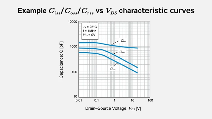
Higher drain voltage widens depletion regions, reducing gate–drain and drain–source capacitances. The datasheet capacitance curves plot each value against drain voltage from 0 V to the rated voltage. In practice, you read capacitance at operating voltages and estimate using average or maximum values. Temperature correction is usually unnecessary unless operating at extreme temperatures.
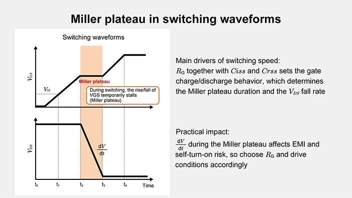
Switching speed depends on the combination of gate-drive resistance, input capacitance, and reverse-transfer capacitance. At turn-on, input capacitance charges until gate voltage exceeds the threshold, then drain voltage falls via the reverse transfer path. Gate voltage temporarily stalls in the Miller region (Miller plateau), and the voltage slew rate (dV/dt) there directly affects EMI and self-turn-on risk.
Reading Capacitance Curves and Balancing Capacitances
Capacitance curves plot input, output, and reverse transfer capacitances from 0 V to the rated drain voltage. The horizontal axis shows drain voltage (log or linear), and the vertical axis shows capacitance on a log scale. Input capacitance often stays relatively flat, while output and reverse transfer capacitances drop as drain voltage rises. You should read values at the operating drain voltage range.
Input capacitance sets the gate driver load. Combine the driver IC’s output capability and the external gate resistance to estimate the charging behavior. The ratio of reverse-transfer capacitance to input-related capacitance indicates the strength of the Miller effect. Larger reverse transfer capacitance makes the Miller plateau longer and increases switching loss. Output capacitance affects drain ringing at turn-off; with inductive loads, it can resonate with stray inductance, leading to ringing that can cause overvoltage stress and radiated noise.
Lower reverse transfer relative to input-related capacitance suppresses the Miller effect, favoring faster switching. Devices with a small Crss relative to Ciss tend to have shorter Miller plateaus and are more resistant to dV/dt-induced self-turn-on in half-bridge configurations.
Total Gate Charge and Miller Plateau
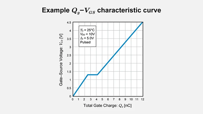
Total gate charge (Qg) is the charge required to transition the MOSFET from off to fully on. A larger Qg means longer charging time and higher switching losses for a given gate drive capability. Datasheets show Qg as a curve of gate voltage versus accumulated charge, and a flat region called the Miller plateau appears where gate voltage rise stalls during drain voltage transition.
Total Charge Definition and On-Resistance Trade-Off
The total gate charge is the time integral of current flowing into the gate, measured in nanocoulombs. Measurement holds drain current and drain voltage at specified values while a constant current charges the gate. The charge accumulated until the gate reaches a specified voltage (e.g., 10 V) is considered the total gate charge.
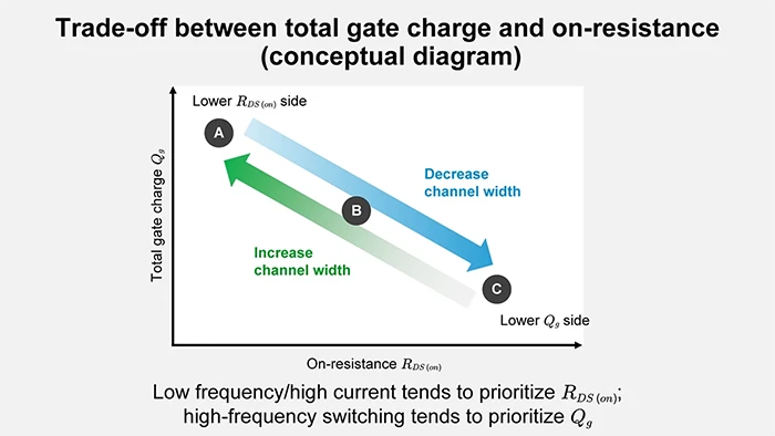
There is a trade-off between total gate charge and on-resistance. Widening the channel reduces on-resistance and lowers conduction loss, but increases gate area, raising input capacitance and total charge, and increasing switching loss. Narrowing the channel raises on-resistance and conduction loss but shrinks total charge and reduces switching loss. High-frequency switching prioritizes low total charge; low-frequency, high-current applications prioritize low on-resistance. In practical design, you choose an optimum balance between conduction and switching losses.
Datasheets may list total charge at multiple drain voltage and current combinations. Higher drain voltage increases Miller-region charge and raises the total gate charge, so you should read Qg at conditions close to your operating drain voltage.
Qg–VGS Curve and the Miller Plateau
The Qg–VGS curve plots accumulated gate charge on the horizontal axis and gate voltage on the vertical axis. Because gate voltage evolves as the gate capacitances are charged, this curve corresponds to the gate-voltage trajectory during switching.
Switching proceeds in three stages. First, gate capacitance charges until the voltage reaches the threshold. Next, gate voltage exceeds the threshold, drain current begins to flow, and drain voltage starts to fall. During the VDS transition, most of the gate current is diverted into Cgd, so VGS stays near the Miller plateau. This flat region is the Miller plateau. Finally, after drain voltage has largely transitioned, gate voltage rises to the final drive level.
During the Miller plateau, drain voltage changes rapidly, and dV/dt becomes large. This slew rate interacts with stray inductance and can produce voltage ringing and radiated EMI. In half-bridges, a fast low-side voltage transition can induce a gate voltage on the high-side device via Crss, causing unintended self-turn-on. The duration of the Miller plateau increases with reverse transfer capacitance and tends to increase at higher drain voltage.
Gate driver design must control Miller-region dV/dt appropriately. Excessive dV/dt worsens EMI and self-turn-on risk; insufficient dV/dt increases switching loss. Gate resistance RG is commonly used to tune switching speed and optimize this trade-off.
Estimating Switching Time from Total Charge
A rough first-order estimate uses the fact that charge equals current multiplied by time. If you approximate an average gate current Igate, then the time to deliver total charge Qg can be estimated as:
\(t≈\displaystyle\frac{Q_g}{I_{gate}}\)
In practical gate-drive loops, the average gate current is set by the effective gate-loop resistance, which includes the external gate resistor, the gate driver output resistance, and wiring/packaging resistances. In the Miller region, the gate voltage tends to “stick” near the Miller plateau voltage, so a useful approximation is that gate current is driven by the difference between the drive voltage and the plateau voltage across the gate-loop resistance. This makes the estimate a starting point rather than a precise prediction, because the real waveform includes the plateau and driver non-idealities.
Switching loss is often approximated by the overlap between drain voltage and drain current during transitions. A common first-order approximation i:
\(P_{sw}≈\displaystyle\frac{V_{DS}×I_D}{2}×(t_r+t_f)×f_{sw}\)
where tr and tf are rise/fall transition times, and fsw is the switching frequency. Because tr and tf scale with the time needed to move charge through the Miller region and the rest of the gate-voltage trajectory, selecting a MOSFET with lower Qg generally reduces switching loss, but often at the cost of higher on-resistance. The design task is to balance conduction loss and switching loss to find the optimum.
Gate Threshold Voltage: Definition and Misconceptions
The gate threshold voltage is the gate voltage at which a conducting channel begins to form between the drain and the source as gate voltage rises and drain current starts to flow. However, datasheet values are measured at a specified tiny current (for example, 1 mA). They do not indicate “the voltage where the MOSFET is fully on.” This misconception is common. In practice, you supply sufficient gate voltage to carry the required load current, while using the threshold voltage primarily to evaluate margin against inadvertent turn-on.
Threshold Definition vs “Turn-On Voltage”
Datasheets typically define threshold voltage by applying specified VDS and measuring the VGS at which the drain current reaches a specified small value. This definition makes threshold the point at which conduction begins, not at which the device can conduct large current with low on-resistance.
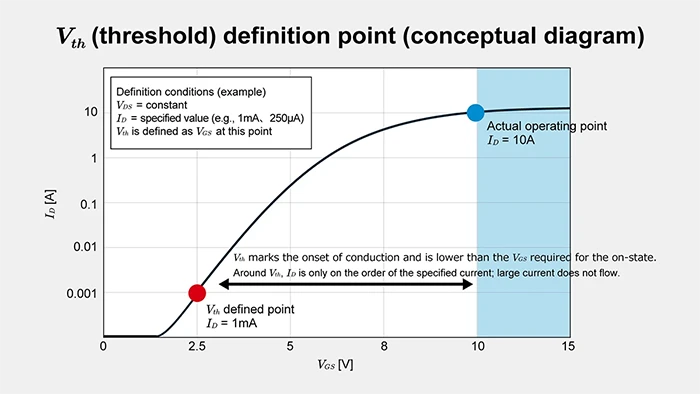
For example, even if a MOSFET has a 2.5 V typical threshold, the transfer characteristics generally show that several volts more gate voltage (often 5–8 V, depending on the device and current level) are needed to conduct large current. Near threshold, only small current flows and the effective on-resistance is much higher than the rated RDS(on). In practical switching circuits, 10–12 V gate drive is common for standard MOSFETs (within VGS(max)); logic-level MOSFETs are driven at the datasheet-recommended VGS for the specified RDS(on).
Threshold variation must also be considered. Datasheets specify minimum, typical, and maximum values, and temperature shifts the threshold as well. For worst-case inadvertent turn-on checks, you typically compare induced gate voltage against the minimum threshold (and, where relevant, the worst-case temperature condition).
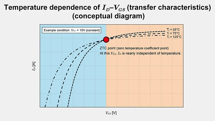
ID–VGS Characteristics, Temperature Dependence, and Temperature Estimation
The drain current versus gate voltage curve (transfer characteristic) is typically shown at a constant drain voltage with multiple temperature curves. Near the threshold, the reduction in threshold voltage with temperature can cause conduction to begin at a lower VGS, so at a fixed VGS, the current can increase as temperature rises. At higher VGS, where the device is strongly enhanced, carrier mobility reduction tends to dominate, and current can decrease with increasing temperature at fixed VGS. The crossover at which the temperature dependence changes sign is often called the zero-temperature-coefficient point (ZTC).
The threshold voltage generally has a negative temperature coefficient (often a few mV/°C in silicon MOSFETs, device- and condition-dependent). Reading the shift on transfer curves can be used as an approximate method to infer temperature change under controlled conditions, though practical circuit estimation must account for many non-idealities.
Practical Threshold Use and Inadvertent Turn-On Margins
In switching design, threshold voltage is most useful as the boundary for inadvertent turn-on margin. In a half-bridge, when one device switches, the other device’s drain voltage slews rapidly, and gate–drain capacitance can couple charge into the gate, raising the gate voltage. If this induced gate voltage exceeds the threshold, the off device can turn on unintentionally, creating shoot-through. This phenomenon is often called self-turn-on.
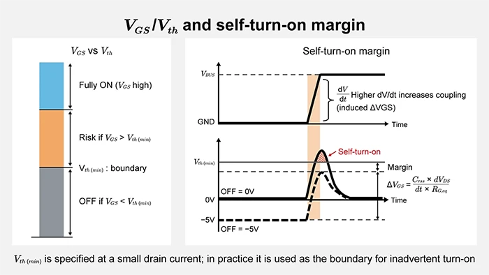
To prevent self-turn-on, you can keep the gate firmly pulled down (lower gate-loop impedance), reduce dV/dt (increase RG appropriately), apply a negative gate voltage for turn-off, or select devices with smaller Crss. A rough scaling is that the coupled current is proportional to Crss × dVDS/dt, and the resulting induced voltage depends on the impedance in the gate loop. In practice, you compare worst-case induced gate voltage to the minimum threshold (with appropriate margin) and choose countermeasures accordingly.
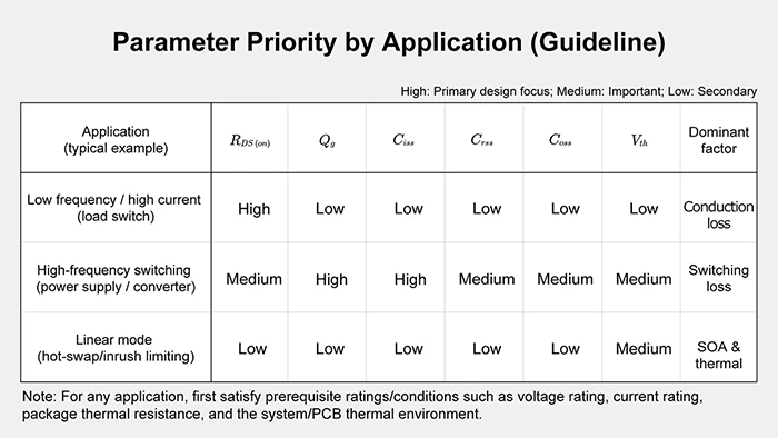
Parameter Selection by Application
Parasitic capacitance, total gate charge, and gate threshold voltage all influence MOSFET switching. Your priorities and acceptable trade-offs depend strongly on operating frequency, current level, and topology.
Parameter Roles and Trade-Offs
Parasitic capacitances directly affect switching speed and ringing. A large input capacitance lengthens gate charge time and increases switching loss for a given driver. Large reverse transfer capacitance strengthens the Miller effect and lengthens the plateau, typically increasing switching loss and influencing dV/dt and EMI. Large output capacitance can increase ringing energy and worsen overvoltage stress and EMI at turn-off.
Total gate charge sets the charge-transfer requirement for switching. Larger Qg increases switching time and switching loss unless the driver can provide proportionally more current. Reducing Qg often increases on-resistance, so conduction and switching losses must be balanced.
Gate threshold voltage sets the lower boundary for channel formation and is critical for inadvertent turn-on margin design. Lower threshold can enable low-voltage drive but can reduce immunity to induced gate voltage. Higher threshold improves immunity but may require higher drive voltage to guarantee full enhancement under all conditions.
Application-Specific Priorities
In low-frequency, high-current load switches, conduction loss often dominates. You tend to prioritize low on-resistance, accepting larger Qg and capacitances if the gate driver can provide sufficient drive and the switching frequency is low enough that switching loss remains secondary.
In high-frequency switching power supplies, switching loss often dominates. You tend to prioritize low Qg and favorable capacitance characteristics, especially smaller reverse transfer capacitance to reduce Miller plateau charge. Output capacitance and the interaction with stray inductance become important for ringing and EMI, and self-turn-on countermeasures may be necessary in half-bridge topologies.
In linear-mode applications such as hot-swap and inrush limiting, the MOSFET spends time with significant VDS and ID simultaneously. Safe operating area and thermal design dominate, and parameter interpretation shifts toward linear control behavior; parasitic capacitance and Qg become secondary to SOA and thermal constraints.
Linear mode (hot-swap or inrush limiting) keeps the MOSFET operating in the saturation region with both drain voltage and current large. Safe operating area and thermal design dominate; parasitic capacitance and total charge are secondary. The interpretation of threshold voltage and transconductance also changes. You linearly control gate voltage to adjust drain current. Linear mode details appear in “MOSFET Linear Mode Basics (Hot-Swap / Inrush).”
Summary
MOSFET switching design starts by extracting parasitic capacitances (Ciss/Coss/Crss), total gate charge (Qg), and gate threshold voltage (VGS(th)) from the datasheet. Input capacitance sets the gate driver load, reverse transfer capacitance creates Miller delay and affects the plateau, and output capacitance influences drain ringing. Their balance shapes switching behavior.
Total gate charge links gate drive capability to switching time and switching loss, and it trades off with on-resistance. Gate threshold voltage is not the “full turn-on voltage” but rather the boundary for channel formation, and it is most valuable for inadvertent turn-on margin checks.
Low-frequency, high-current applications often prioritize on-resistance. High-frequency switching prioritizes total gate charge and favorable capacitance characteristics, especially smaller reverse transfer capacitance. Reading capacitance curves and Qg–VGS curves at operating conditions provides a practical starting point for estimating switching behavior and selecting gate resistance, which you then refine with loss, thermal, and SOA considerations.
Related Articles
“Transistor Fundamentals”
“Bipolar Junction Transistor (BJT) Basics”
【Download Documents】 Basics of Si Power Devices
In this handbook, although there are so many types of power devices using Si semiconductors, the basic points are explained, focusing mainly on diodes and transistors for power supply applications. It also introduces the procedure and decision method for transistor selection when designing circuits, as well as application examples that utilize each characteristic and feature.

Transistors
Basic
-
Basics of Transistors
- Transistor Fundamentals: Structure, Types, and Operating Principles
- Bipolar Junction Transistor (BJT) Basics: Operation and Applications (NPN & PNP)
- NPN Transistor: Low-Side Switch Fundamentals
- PNP Transistor: High-Side Switch Fundamentals
- MOSFET Basics: Parasitic Capacitance, Gate Charge, Miller Region, and Threshold Voltage
- MOSFET On-Resistance (RDS(on))
- Super junction MOSFET (SJ MOSFET) Basics
- What is a Digital Transistor?
- Digital Transistor Selection
- How to select<Selecting Transistors to Ensure Safe Operation>
- Junction Temperature <Calculating Transistor Chip Temperature>
- What is a Load Switch?
- Basics of MOSFETs
- Introduction
-
Confirming the Suitability of a Transistor in Actual Operation – Introduction
- Confirmation of the Chip Temperature
- Confirmation of Suitability in Actual Operation and Preparations
- Confirmation that Absolute Maximum Ratings are Satisfied
- Confirmation that Operation is within the SOA (Safe Operating Area)
- Confirmation that Operation is within the SOA Derated at the Actual Operating Temperature
- Confirmation that Average Power Consumption is within the Rated Power
- Summary
- Summary
Evaluation
-
The Importance of the Recovery Characteristics of Primary-side Switching Elements in LLC Converters -Introduction-
- Basic Configuration of an LLC Converter
- Features of LLC Converter Operation
- Basic Operation of LLC Converters
- Importance of MOSFET Recovery Characteristics for Off-Resonance of LLC Converters
- The Importance of the Recovery Characteristics of Primary-side Switching Elements in LLC Converters ーSummaryー
-
The Importance of the Reverse Recovery Characteristics of Switching Elements in Inverter Circuits -Introduction-
- Types of Inverter Circuits and Energization Methods
- Basic Operation of 3-Phase Modulation Inverter Circuits
- Comparison of Losses in a PrestoMOS™ MOSFET and a Standard SJ MOSFET Using Double-Pulse Tests (Actual Measurement Results)
- Comparison of Efficiency of a PrestoMOS™ MOSFET and a Standard SJ MOSFET in a 3-Phase Modulation Inverter Circuit (Simulations)
- The Importance of the Reverse Recovery Characteristics of Switching Elements in Inverter Circuits -Summary-
- Mechanisms of MOSFET Destruction
- About Double-Pulse Tests
-
Improving the Power Conversion Efficiency of Phase Shift Full Bridge Circuits – Introduction
- Basic Configuration of a PSFB Circuit
- Basic Operation of PSFB Circuits
- Guidelines Relating to Operation of Switching Elements Under Light Loading
- Guidelines Relating to Operation of Switching Elements Under Heavy Loading
- Evaluation of Efficiency
- Improving the Power Conversion Efficiency of Phase Shift Full Bridge Circuit – Summary –