Transistors|Basic
Summary
2018.05.10
In this chapter, we have explained methods and procedures for determining whether or not a selected transistor is appropriate in actual operation. This final article ends with “Summary”.
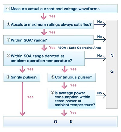
The flowchart on the right and the list of procedures below were followed to check whether selected transistors are appropriate for the actual operating conditions, and to confirm operation under conditions for which sufficient reliability and safety are secured.
- ① Measurement of the actual current and voltage waveforms
- ② Confirmation that absolute maximum ratings are satisfied
- ③ Confirmation that operation is within the SOA (safe operating area)
- ④ Confirmation that operation is within the SOA derated at the ambient operating temperature
- ⑤ Continuous pulses (switching operation)
- ⑥ Confirmation that average power consumption is within the rated power
- ⑦ Confirmation of the chip temperature
Below, key points indicated for each of the procedures in the list are summarized.
①Measurement of the actual current and voltage waveforms
Key Points:
・In prototyping, it is essential to determine whether a selected transistor can be used in actual operation.
・For purposes of confirmation, the voltages and currents handled by the transistor are measured.
②Confirmation that absolute maximum ratings are satisfied
Key Points:
・Correctly understand the definition and purpose of absolute maximum ratings, and learn to judge whether a component can be used.
③Confirmation that operation is within the SOA (safe operating area)
Key Points:
・The SOA (Safe Operating Area) is information used to confirm that a transistor is operating under safe conditions.
・In essence, in a graph of the relationship between ID and VDSS, the SOA indicates the safe area of operation with respect to the rated voltage and current and the allowable power dissipation (heat generation).
・The SOA conditions should be checked carefully, and differences with actual usage conditions should be considered, prior to device use.
④Confirmation that Operation is within the SOA Derated at the Ambient Operating Temperature
Key Points:
・An SOA graph is for data at Ta=25°C, and so the SOA must be derated according to the temperature at which the transistor will actually be used.
・As the derating rate, the derating rate for allowable power dissipation is used.
⑤Continuous pulses (switching operation)
⑥Confirmation that Average Power Consumption is within the Rated Power
Key Points:
・In the case of continuous-pulse (switching) operation, the average power consumption is determined, and it is confirmed that allowable power dissipation is within the rated value.
・A judgment will in the end depend on whether Tj exceeds the absolute maximum rating.
⑦Confirmation of the Chip Temperature
Key Points:
・It should be confirmed that Tj ultimately does not exceed the absolute maximum rating.
・Tj is the sum of Ta or Tc and the heat generation (the product of the thermal resistance and the power consumption).
This concludes the discussion of “Confirmation of Suitability in Actual Operation and Preparations”. Executing each of the separate procedures is rather troublesome, but it should be understood that these processes are an unavoidable part of circuit design.
【Download Documents】 Basics of Si Power Devices
In this handbook, although there are so many types of power devices using Si semiconductors, the basic points are explained, focusing mainly on diodes and transistors for power supply applications. It also introduces the procedure and decision method for transistor selection when designing circuits, as well as application examples that utilize each characteristic and feature.

Transistors
Basic
-
Basics of Transistors
- Transistor Fundamentals: Structure, Types, and Operating Principles
- Bipolar Junction Transistor (BJT) Basics: Operation and Applications (NPN & PNP)
- NPN Transistor: Low-Side Switch Fundamentals
- PNP Transistor: High-Side Switch Fundamentals
- MOSFET Basics: Parasitic Capacitance, Gate Charge, Miller Region, and Threshold Voltage
- MOSFET On-Resistance (RDS(on))
- Super junction MOSFET (SJ MOSFET) Basics
- What is a Digital Transistor?
- Digital Transistor Selection
- How to select<Selecting Transistors to Ensure Safe Operation>
- Junction Temperature <Calculating Transistor Chip Temperature>
- What is a Load Switch?
- Basics of MOSFETs
- Introduction
-
Confirming the Suitability of a Transistor in Actual Operation – Introduction
- Confirmation of the Chip Temperature
- Confirmation of Suitability in Actual Operation and Preparations
- Confirmation that Absolute Maximum Ratings are Satisfied
- Confirmation that Operation is within the SOA (Safe Operating Area)
- Confirmation that Operation is within the SOA Derated at the Actual Operating Temperature
- Confirmation that Average Power Consumption is within the Rated Power
- Summary
- Summary
Evaluation
-
The Importance of the Recovery Characteristics of Primary-side Switching Elements in LLC Converters -Introduction-
- Basic Configuration of an LLC Converter
- Features of LLC Converter Operation
- Basic Operation of LLC Converters
- Importance of MOSFET Recovery Characteristics for Off-Resonance of LLC Converters
- The Importance of the Recovery Characteristics of Primary-side Switching Elements in LLC Converters ーSummaryー
-
The Importance of the Reverse Recovery Characteristics of Switching Elements in Inverter Circuits -Introduction-
- Types of Inverter Circuits and Energization Methods
- Basic Operation of 3-Phase Modulation Inverter Circuits
- Comparison of Losses in a PrestoMOS™ MOSFET and a Standard SJ MOSFET Using Double-Pulse Tests (Actual Measurement Results)
- Comparison of Efficiency of a PrestoMOS™ MOSFET and a Standard SJ MOSFET in a 3-Phase Modulation Inverter Circuit (Simulations)
- The Importance of the Reverse Recovery Characteristics of Switching Elements in Inverter Circuits -Summary-
- Mechanisms of MOSFET Destruction
- About Double-Pulse Tests
-
Improving the Power Conversion Efficiency of Phase Shift Full Bridge Circuits – Introduction
- Basic Configuration of a PSFB Circuit
- Basic Operation of PSFB Circuits
- Guidelines Relating to Operation of Switching Elements Under Light Loading
- Guidelines Relating to Operation of Switching Elements Under Heavy Loading
- Evaluation of Efficiency
- Improving the Power Conversion Efficiency of Phase Shift Full Bridge Circuit – Summary –