Transistors|Basic
Super junction MOSFET (SJ MOSFET) Basics
2026.06.22
table of contents
- ・Where SJ MOSFETs Fit Among Power Transistors
- ・Differences Between Planar MOSFETs and SJ MOSFETs
- ・How Structural and Design Differences Show Up in Device Characteristics
- ・Design Targets and Typical Trade-Offs
- ・How to Decide Whether an External Fast-Recovery Diode Is Needed
- ・What to Prioritize in the Datasheet
- ・Summary
A superjunction MOSFET (SJ MOSFET) is a silicon power MOSFET that achieves high breakdown voltage while maintaining lower on-resistance than conventional planar silicon MOSFETs of similar voltage rating. It is particularly valuable in offline AC/DC power supplies, PFC stages, LLC converters, flyback converters, and a wide range of industrial power applications, where both higher efficiency and smaller size are important. This article examines how differences in device structure and design optimization manifest as characteristics such as low noise, fast switching, short trr (reverse recovery time), and low Qrr (reverse recovery charge), and the trade-offs behind those characteristics.
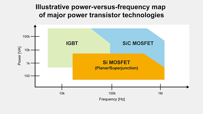
Where SJ MOSFETs Fit Among Power Transistors
When selecting a power transistor, you need to evaluate the voltage and current ratings, switching frequency, efficiency, cost, and practical implementation. IGBTs are strong in high-voltage, high-power applications, while SiC MOSFETs extend more easily into higher-voltage, higher-temperature, and higher-frequency ranges. Si MOSFETs, on the other hand, offer a strong balance between ease of high-frequency operation and cost. Among them, the SJ MOSFET is especially important because it greatly relaxes the traditional trade-off found in conventional Si MOSFETs, particularly planar MOSFETs with a uniform drift region, where higher breakdown voltage comes at the cost of higher on-resistance (RDS(on)). As a result, SJ MOSFETs play an important role in Si devices in the 600 V to 800 V class.
Keep in mind that the familiar power-versus-frequency map for power transistors can shift significantly depending on topology, cooling conditions, efficiency targets, and allowable system cost.
Differences Between Planar MOSFETs and SJ MOSFETs
In a planar MOSFET, the drift region supports the blocking voltage when the device is off. To increase breakdown voltage, the drift region must be made both thicker and more lightly doped. However, the resistance of that drift region directly contributes to RDS(on), so there is a practical limit to how far you can push both higher voltage capability and lower on-resistance at the same time. When channel conduction dominates, conduction loss can be approximated as Pcond ≈ I_rms^2 × RDS(on), so any increase in RDS(on) translates directly into higher loss.
An SJ MOSFET takes a different approach. It forms alternating n-type and p-type pillars in the drift region. In the off-state, the charges in those pillars compensate each other, allowing the depletion region to expand laterally and vertically. This charge-balance concept makes it possible to maintain high breakdown voltage even with a more heavily doped drift region than in a planar structure. As a result, for the same voltage rating, RDS(on) can be reduced, or for the same RDS(on), chip size can be reduced. That is the essential advantage of the SJ MOSFET.
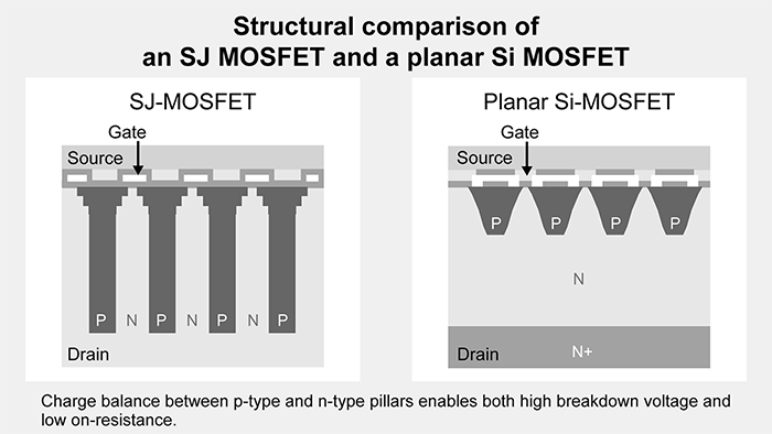
At the same time, the SJ structure is more difficult to manufacture, and if the charge balance between the p-pillars and n-pillars is not well controlled, the expected benefits in breakdown voltage and on-resistance cannot be fully realized. Also, while achieving the same RDS(on) with a smaller chip can help reduce total gate charge Qg and output capacitance Coss, thermal margin and robustness under abnormal conditions need to be evaluated separately. In particular, avalanche-related robustness and limits specified under UIS conditions must be compared carefully and under equivalent conditions. In other words, the SJ MOSFET is not simply a device that makes everything better. It is a device whose real value depends on how its characteristics are optimized and how well it is applied.
For explanations of MOSFET-specific parameters, see the articles below.
MOSFET Basics | Parasitic Capacitances, Qg, Miller Plateau, and Threshold Voltage
MOSFET On-Resistance (RDS(on))
How Structural and Design Differences Show Up in Device Characteristics
One of the key points about SJ MOSFETs is that even devices based on the same superjunction concept can behave quite differently depending on the design target. Manufacturers tune cell structure, gate structure, and surrounding cell layout, internal gate resistance, the behavior of gate-drain capacitance Cgd and output capacitance Coss, body diode design and adjacent device structure, and, especially for reverse-recovery behavior, carrier lifetime control to steer device behavior toward low noise, fast switching, or short trr and low Qrr. These characteristics are not independent, however. Pushing one of them harder usually means accepting trade-offs somewhere else.
Design Optimized for Low Noise
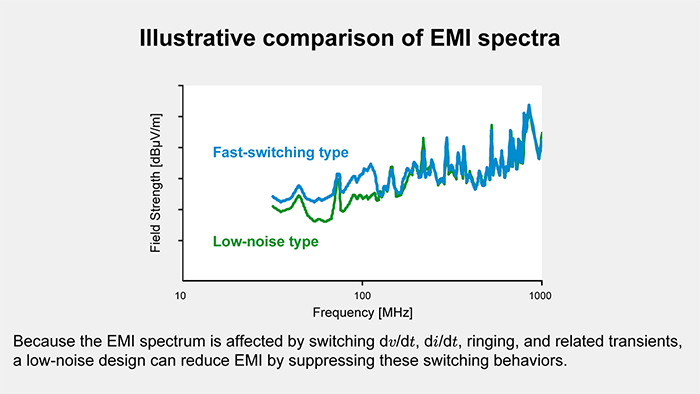
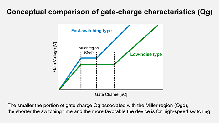
The basic idea behind a low-noise design is to avoid making dv/dt and di/dt any steeper than necessary during switching. To do that, designers tune parameters such as the gate-drain charge Qgd and the effective behavior of Cgd in the Miller region, and may also optimize the internal gate resistance to better control voltage and current transitions.
The benefit of this kind of optimization is that both radiated and conducted noise are easier to suppress. It also tends to reduce drain-voltage overshoot, ringing, and false turn-on, making the circuit more forgiving of PCB layout and gate-drive conditions.
The trade-off is that a design optimized for lower noise is, by nature, also somewhat slower-switching. Turn-on and turn-off losses therefore tend to increase, reducing the margin available for higher-frequency operation under the same thermal design. Low-noise behavior is valuable in its own right, but it should be understood as a characteristic that comes at the expense of efficiency.
Design Optimized for Fast Switching
Devices optimized for fast switching are designed to reduce Qg and Qgd, lower internal gate resistance, and minimize internal parasitic elements and parasitic effects that degrade switching behavior. If you use Qg at the actual gate-drive voltage, gate-drive loss generally increases with switching frequency, as Pgate ≈ Qg × Vg × fsw, so reducing Qg becomes especially important at high switching frequencies. Also, the smaller Qgd is, the shorter the Miller interval becomes, making it easier to speed up turn-on and turn-off transitions.
This design makes it easier to reduce switching losses, improving power-supply efficiency and enabling the use of smaller magnetics. It is especially attractive in applications targeting better light-load to mid-load efficiency or higher power density through higher switching frequency.
The downside is that dv/dt and di/dt tend to increase, making the circuit more sensitive to parasitic inductance and capacitance. That makes issues such as drain-voltage overshoot, source bounce, gate ringing, worse EMI, and false turn-on of the complementary device more likely to appear. Even if a fast-switching device looks attractive in datasheet metrics, its real performance depends heavily on PCB layout, gate resistance, driver capability, and current-return-path design.
Design Optimized for Short trr and Low Qrr
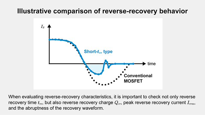
In half-bridge and full-bridge circuits, totem-pole PFC stages, and motor drives, there are cases where the MOSFET body diode participates in commutation. In these situations, what matters is not just whether trr is short. You also need to look at the reverse recovery charge Qrr, the peak reverse recovery current Irrm, and the softness or snappiness of the recovery waveform.
Design optimization for short trr and low Qrr reduces carrier storage near the body diode and optimizes lifetime and recombination, thereby reducing the charge that the complementary device must pull out when it turns on. This can help reduce commutation loss and transient stress. Under the right conditions, it can also reduce the need for an external fast-recovery diode (FRD).
There is, however, an important caveat. Depending on the application, the body diode of an SJ MOSFET can still be subjected to severe hard-commutation stress when the complementary device turns on after the body diode has been conducting. Even if trr is short, a large Irrm can still make noise and voltage spikes difficult to control. Even if Qrr is small, a waveform that cuts off very abruptly can still excite ringing. For that reason, suitability should not be judged solely by the claim of short trr. Qrr, Irrm, test conditions, and actual switching waveforms all need to be checked.
Design Targets and Typical Trade-Offs
Even among SJ MOSFETs, the parameters that matter most, along with the practical design considerations surrounding them, vary depending on the characteristic the device was optimized for. The overall picture is summarized below.
| Target characteristic | Key parameters to check | Benefits | Main trade-offs |
| Low noise | Qgd, effective Cgd, internal gate resistance, dv/dt | Lower EMI, reduced overshoot and ringing, easier implementation | Switching loss tends to increase, and the margin for higher-frequency operation tends to shrink |
| Fast switching | Qg, Qgd, internal gate resistance, Eon / Eoff | Higher efficiency, higher-frequency operation, smaller magnetics | Larger dv/dt and di/dt, worse EMI, false turn-on, greater layout sensitivity |
| Short trr / low Qrr | trr, Qrr, Irrm, recovery-waveform softness/snappiness | Lower commutation loss, reduced stress on the complementary device, and a better chance of eliminating the FRD | Depending on conditions, hard-commutation stress may remain, so hardware verification is essential |
How to Decide Whether an External Fast-Recovery Diode Is Needed
Why Is an External Fast-Recovery Diode (FRD) Used?
In bridge circuits such as inverters and motor drives, the body diode may conduct during dead time or regenerative operation, and the complementary device may turn on immediately afterward. In that case, the charge stored in the diode must be removed quickly, which creates a reverse recovery current. Because the complementary device must carry that reverse recovery current in addition to the load current, commutation loss, voltage overshoot, ringing, and EMI all tend to increase.
For that reason, if the body diode’s reverse recovery behavior is inadequate, designers may add an external FRD in anti-parallel with the MOSFET to reduce reverse-recovery-related switching losses and noise. The downside is that the added FRD increases part count, board area, cost, and parasitics. In addition, whenever the diode actually conducts, its forward voltage drop also contributes to loss.
When It Is Easier to Eliminate the External Fast-Recovery Diode
It becomes easier to eliminate the external FRD when the selected SJ MOSFET has sufficiently low Qrr and Irrm, and when the circuit conditions do not force the body diode into deep or long-duration conduction. Examples include circuits with commutation close to soft switching, designs with well-controlled dead time, and implementations with parasitic inductance kept low. In such cases, the built-in body diode may be sufficient.
On the other hand, if hard commutation occurs frequently, or if current, temperature, and switching frequency are all high, eliminating the external FRD becomes much more difficult. For that reason, you should not generalize from the statement, “This device has short trr, so no FRD is needed.” The first step is to understand how long the body diode conducts in the target circuit and at what current.
Points to Watch When Deciding Whether an FRD Is Required
When deciding whether an external FRD is needed, it is important not to conclude datasheet trr or Qrr values alone. These values vary significantly with forward current IF, current slew rate di/dt, and junction temperature Tj. Any comparison must be made under identical test conditions. In the end, voltage spikes, ringing, thermal behavior, and EMI should be checked using double-pulse testing and actual switching waveforms on real hardware.
What to Prioritize in the Datasheet
Selecting an SJ MOSFET is not just about looking at on-resistance alone. At a minimum, you need to consider conduction loss, gate-drive loss, switching speed, commutation loss and noise, and overall robustness.
First, RDS(on) is the basic indicator for conduction loss. But it is not enough to look only at the typical value at 25°C. You also need to examine how much it increases at elevated temperature and what that means at your actual operating current. Even at the same voltage rating and in the same package, different product families can balance RDS(on) and Qg quite differently, so figures of merit such as RDS(on) × Qg are also useful for comparison.
Next, check Qg, Qgd, the internal gate resistance, and, when available, Eon and Eoff. Qgd strongly influences the Miller interval, so total Qg alone is not enough; what matters is how the charge is distributed. Faster devices often give you more room to tune behavior with external gate resistance, but they also become more layout-sensitive.
If the circuit may rely on the body diode, then trr, Qrr, and Irrm should be high-priority parameters. Here, matching test conditions is absolutely essential. Also, whether the waveform is abrupt and whether it tends to ring are not always clear from a parameter table alone, so it is worth checking characteristic curves and application notes as well.
For SJ MOSFETs, the strong voltage dependence of Coss is another point that should not be overlooked. A single small-signal Coss value does not always capture turn-on energy or ringing tendency well enough. When available, output charge Qoss and stored output energy Eoss can provide a comparison that is closer to actual circuit behavior. This is particularly important in resonant topologies and in designs where light-load efficiency matters.
Finally, it is also necessary to check robustness under abnormal conditions, including surge capability, avalanche-related robustness, and limits specified under UIS conditions. SJ MOSFETs offer major benefits in reduced loss, but design margin under abnormal circuit conditions is a separate issue. A good device choice should account not only for normal-operation efficiency, but also for the stress the device will see during startup, shutdown, inrush, and fault events.
Summary
Selecting an SJ MOSFET is not simply a matter of choosing the MOSFET with the lowest on-resistance. It is the process of translating key circuit-design priorities into device-selection criteria: how much noise can be tolerated, how much switching speed is needed, and how critically body-diode reverse recovery must be treated.
In that sense, low-noise, fast-switching, and short- trr /low- Qrr variants are better understood not just as different product labels, but as distinct points in the design space defined by structural and optimization choices. The most important part of using SJ MOSFETs well is correlating datasheet numbers with actual switching waveforms and finding the best balance among efficiency, noise, and robustness.
Related article:
MOSFET Basics | Parasitic Capacitances, Qg, Miller Plateau, and Threshold Voltage
MOSFET On-Resistance (RDS(on))
【Download Documents】 Basics of Si Power Devices
In this handbook, although there are so many types of power devices using Si semiconductors, the basic points are explained, focusing mainly on diodes and transistors for power supply applications. It also introduces the procedure and decision method for transistor selection when designing circuits, as well as application examples that utilize each characteristic and feature.

Transistors
Basic
-
Basics of Transistors
- Transistor Fundamentals: Structure, Types, and Operating Principles
- Bipolar Junction Transistor (BJT) Basics: Operation and Applications (NPN & PNP)
- NPN Transistor: Low-Side Switch Fundamentals
- PNP Transistor: High-Side Switch Fundamentals
- MOSFET Basics: Parasitic Capacitance, Gate Charge, Miller Region, and Threshold Voltage
- MOSFET On-Resistance (RDS(on))
- Super junction MOSFET (SJ MOSFET) Basics
- What is a Digital Transistor?
- Digital Transistor Selection
- How to select<Selecting Transistors to Ensure Safe Operation>
- Junction Temperature <Calculating Transistor Chip Temperature>
- What is a Load Switch?
- Basics of MOSFETs
- Introduction
-
Confirming the Suitability of a Transistor in Actual Operation – Introduction
- Confirmation of the Chip Temperature
- Confirmation of Suitability in Actual Operation and Preparations
- Confirmation that Absolute Maximum Ratings are Satisfied
- Confirmation that Operation is within the SOA (Safe Operating Area)
- Confirmation that Operation is within the SOA Derated at the Actual Operating Temperature
- Confirmation that Average Power Consumption is within the Rated Power
- Summary
- Summary
Evaluation
-
The Importance of the Recovery Characteristics of Primary-side Switching Elements in LLC Converters -Introduction-
- Basic Configuration of an LLC Converter
- Features of LLC Converter Operation
- Basic Operation of LLC Converters
- Importance of MOSFET Recovery Characteristics for Off-Resonance of LLC Converters
- The Importance of the Recovery Characteristics of Primary-side Switching Elements in LLC Converters ーSummaryー
-
The Importance of the Reverse Recovery Characteristics of Switching Elements in Inverter Circuits -Introduction-
- Types of Inverter Circuits and Energization Methods
- Basic Operation of 3-Phase Modulation Inverter Circuits
- Comparison of Losses in a PrestoMOS™ MOSFET and a Standard SJ MOSFET Using Double-Pulse Tests (Actual Measurement Results)
- Comparison of Efficiency of a PrestoMOS™ MOSFET and a Standard SJ MOSFET in a 3-Phase Modulation Inverter Circuit (Simulations)
- The Importance of the Reverse Recovery Characteristics of Switching Elements in Inverter Circuits -Summary-
- Mechanisms of MOSFET Destruction
- About Double-Pulse Tests
-
Improving the Power Conversion Efficiency of Phase Shift Full Bridge Circuits – Introduction
- Basic Configuration of a PSFB Circuit
- Basic Operation of PSFB Circuits
- Guidelines Relating to Operation of Switching Elements Under Light Loading
- Guidelines Relating to Operation of Switching Elements Under Heavy Loading
- Evaluation of Efficiency
- Improving the Power Conversion Efficiency of Phase Shift Full Bridge Circuit – Summary –