Transistors|Basic
PNP Transistor: High-Side Switch Fundamentals
2026.03.09
table of contents
- ・Role and Applications of PNP Transistors (Bipolar Junction Transistors)
- ・Basic PNP Transistor Wiring (High-Side Switch)
- ・High-Side Switch Operation Criteria (Focus on “Ensuring Turn-Off”)
- ・Wiring and Protection Techniques for Safe, Stable Operation
- ・Common High-Side Drive Problems and Solutions
- ・Summary
A PNP transistor is a bipolar junction transistor used in switching applications as a high-side device where current flows from emitter to collector. PNP transistors are commonly used as high-side switches that supply current from the supply rail (+V) to loads. Unlike NPN transistors, PNP transistors turn on when the base is at a lower potential than the emitter and turn off when the base is returned to the emitter potential. Without a proper understanding of this operating principle, wiring errors can cause problems such as loads remaining dimly lit or failing to turn off completely.
This article covers the basic wiring configuration for using PNP transistors as high-side switches, base-handling methods to ensure reliable turn-off, diode placement to protect inductive loads, and standard troubleshooting methods for common issues. We also demonstrate how to trace current flow from circuit symbol arrows to prevent polarity errors.
Notation (sign convention)
In this article, VBE, VCE(sat), and VCE are treated as positive voltage drops (magnitudes) between terminals. In equations, we write | VBE|, | VCE(sat)|, and | VCE| explicitly. Under the strict definitions (VBE = VB − VE, VCE = VC − VE), these values become negative during normal PNP conduction. Some datasheets use VEB = VE − VB and VEC = VE − VC; in that case, VEB = | VBE| and VEC = | VCE| in this article.
Role and Applications of PNP Transistors (Bipolar Junction Transistors)
PNP transistors are chosen for high-side switching because they can supply current directly from the supply rail to the load while stabilizing the load-side potential. The PNP bipolar transistor functions as an amplifier, with a small base current controlling a large emitter-to-collector current in current‑sourcing configuration. We describe conventional current flow; electron flow is in the opposite direction. In active mode, the DC gain (hFE, β) relates a small base current to a larger collector current, while the emitter current equals the sum of base and collector currents. With the emitter connected to +V, the collector node rises to approximately supply voltage minus |VCE(sat)| when the transistor is used as a switch (i.e., driven into saturation). When off, the collector becomes high impedance, and the load current becomes nearly zero. Understanding the differences between NPN and low-side configurations helps determine the appropriate circuit topology.
Why PNP is Used in High-Side Switches
High-side PNP transistor placement is preferred because it connects the load’s positive side directly to the supply voltage while stabilizing the load-side potential. PNP turns on when the base voltage is lower than the emitter voltage and turns off when they are equal. This polarity makes PNP attractive for switching applications that keep the load at a defined positive potential. PNP transistors turn on by pulling the base voltage to a lower potential than the emitter, performing current‑sourcing configuration that supplies collector current from emitter to collector, with the emitter connected to +V. On, the collector supplies a voltage equal to the supply voltage minus |VCE(sat)|. When off, the collector becomes high impedance, and the load current becomes nearly zero.
For example, when driving a 12 V, 80 mA relay with a general-purpose PNP transistor, setting forced β to 10 gives Ib ≈ 8 mA. Pulling the driver side of the base resistor to 0 V forward-biases the base-emitter junction, so the junction clamps at approximately | VBE|≈ 0.7 V, with the remaining voltage (approximately 11.3 V) dropping across the base resistor. The base resistor initial value is RB ≈ (12 − 0.7)/0.008 ≈ 1.4 kΩ. With |VCE(sat)| around 0.2 V, Collector-emitter dissipation is approximately 0.2 × 0.08 = 16 mW.
(This 16 mW is the collector–emitter dissipation only; the total transistor dissipation is slightly higher when the base term |VBE|×IB is included.)
However, if the microcontroller is powered from 5 V while the load supply is 12 V, direct base drive is unsafe and may not fully turn the PNP off. When the MCU output is HIGH (5 V) or high‑impedance, the base can still be far below the emitter (12 V), so the BE junction may remain forward‑biased and the load may stay on or dimly lit. In addition, the base node can be pulled toward approximately VE − | VBE(on)|, which can drive current through the base resistor into the MCU pin / VDD (injection / back‑powering) and exceed the controller’s limits. When supply voltages differ, use a level‑shifter (e.g., an NPN transistor) as described in the “Ensuring Turn‑Off” section.
In contrast, low-side configurations pull the load’s negative side to ground, keeping the load’s positive side always connected to the supply voltage. High-side switching suits cases where the load’s negative side must be maintained at an arbitrary potential or where multiple loads share a common ground. Even when the microcontroller and load supply voltages match, PNP transistors require special attention during wiring design due to their inverted control polarity.
For a comprehensive overview of bipolar junction transistors, see Bipolar Junction Transistor (BJT) Basics: Operation and Applications (NPN & PNP)
Key Differences Between NPN (Low-Side) Switches
The differences between NPN and PNP transistors appear in the direction of current flow and the polarity of the control voltage. Incorrect emitter connections prevent proper turn-off or cause damage through reverse bias.
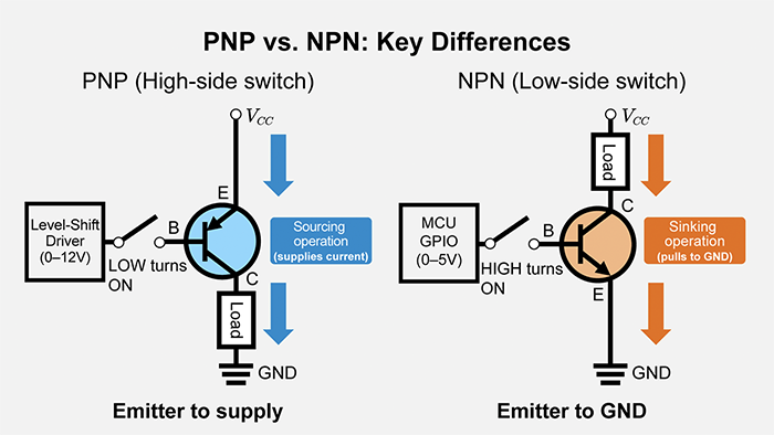
- PNP performs a current sourcing configuration, supplying output current to loads; NPN performs a sink operation, pulling loads to ground
- PNP turns on when the base voltage is lower than the emitter (L level equivalent); NPN turns on at the H level (inverted control polarity)
- In switching applications, the PNP high‑side switch connects the emitter to +V, whereas the NPN low‑side switch connects the emitter to GND.
Understanding these differences enables proper selection between high-side and low-side topologies. For NPN transistor details, see NPN Transistor: Low-Side Switch Fundamentals.
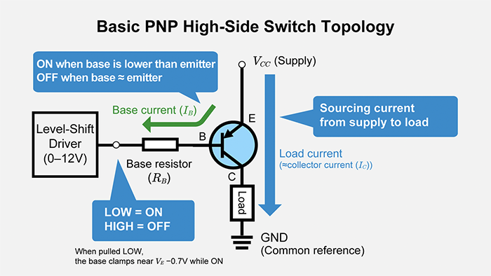
Basic PNP Transistor Wiring (High-Side Switch)
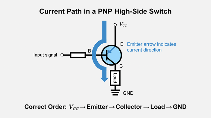
The primary cause of high-side wiring failures is incorrect current path sequencing and emitter potential errors. In proper PNP transistor circuits, current flows in this sequence: Supply → Emitter → Collector → Load → Ground. Connecting the emitter to the ground side prevents proper turn-on or causes unintended current flow. The emitter arrow indicates the direction of conventional current (it points inward for a PNP). Electron flow is opposite to the arrow direction. In open-collector (PNP source output) configurations, attention is required to handle load-side potential.
Basic Wiring Configuration and Current Flow (+V → PNP → Load → GND)
High-side switch wiring has only one correct sequence: Supply (+V) → Emitter → Collector → Load → Ground. When the PNP is on, current flows into the emitter and out of the collector to the load, driving it. In the off state, the base current becomes zero, and the emitter-collector path is cut off.
Reversing this sequence severely degrades the characteristics and increases the risk of damage. An emitter-collector reverse connection results in reverse-mode operation, where current gain is orders of magnitude lower than in forward mode, and breakdown voltage ratings may not be guaranteed. This is not recommended even for temporary evaluation connections. If the emitter is mistakenly tied to the low side (near GND), the circuit will not behave as a high side switch and the intended control may fail. Depending on load placement, unintended current can flow through internal junctions (e.g., the base collector diode), which may partially power the load or back power the controller.
Preventing Polarity Errors with Symbol Arrows
In PNP transistor symbol diagrams, the emitter arrow points inward (toward the transistor body). The arrow shows the direction of conventional current; electron motion is in the opposite direction. This arrow indicates traditional current flow (inward for PNP, outward for NPN). The transistor symbol arrow indicates polarity at the base and emitter terminals. It’s unrelated to +V direction. Confirming this arrow direction prevents confusion with NPN transistors.
Misreading arrow direction leads to emitter-collector confusion. For detailed symbol definitions, see Bipolar Junction Transistor (BJT) Basics: Operation and Applications (NPN & PNP).
Open-Collector (PNP Source Output) Considerations
In PNP source output configurations, the emitter is connected to the supply voltage (+V), and the collector drives the load. The load’s other terminal connects to ground. When the transistor turns on, emitter current flows from the emitter through the transistor into the collector and then through the load to ground, so the collector node rises to approximately +V − |VCE(sat)|. When off, the collector becomes high-impedance, and the load current approaches zero (verify leakage currents ICEO and ICEX in the datasheets; these increase with temperature, requiring threshold settings for high-impedance interpretation). At high temperatures, leakage currents can make LEDs appear dimly lit even when ‘off’.
This configuration suits DC loads such as relay coils and LEDs (add flyback protection for inductive loads). The output current delivered to the load depends on the base input voltage and available voltage sources; Ensure the base drive never forces the MCU pin above VDD (injection/back-powering). Keep the pin within the MCU’s absolute maximum ratings. With the load’s ground side shared with other circuits, wiring becomes simpler. When a microcontroller and a load share the same ground, no separate ground line routing is needed. However, when the microcontroller and load supply voltages differ, attention is required to level-shift the base drive circuit.
High-Side Switch Operation Criteria (Focus on “Ensuring Turn-Off”)
Switch operation success depends on controlling the PNP transistor between cutoff, active, and saturation modes. In active mode, the base-emitter junction is forward-biased, and the collector-base junction is reverse-biased. Conversely, in saturation mode, both junctions are forward-biased, and the transistor conducts the required load current with a low | VCE(sat)|. The actual current is determined by the base drive, the load, and the device’s maximum ratings. In cutoff, the base-emitter junction (BE junction) isn’t forward-biased, and the collector current remains nearly zero. In saturation mode, the transistor exhibits low resistance as |VCE| decreases, thereby minimizing the emitter-collector resistance. In active mode, the BE junction is forward-biased while the base-collector junction (BC junction) remains reverse-biased, providing current gain but unsuitable for switching. For high-side switches, “ensuring turn-off” requires particular attention. When the base floats or has insufficient potential difference with respect to the emitter, the transistor cannot fully turn off, and a small current continues to flow to the load. Understanding the relationships between base voltage, base-emitter voltage (|VBE|), |VCE(sat)|, and collector current enables definitive condition setting.
On/Off Conditions and Base Voltage Relationship (Pulling Base Lower Than Emitter)
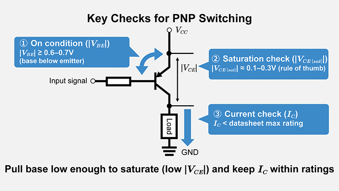
Switch operation pass/fail is determined by three parameters: |VBE|, |VCE(sat)|, and collector current (IC). These parameters serve as criteria for distinguishing cutoff from saturation states. Key checks: |VBE| ≈ 0.6–0.7 V when forward-biased, |VCE(sat)| low in saturation, collector current within ratings, current gain used only for estimation.
- |VBE| (Base-Emitter Voltage magnitude): For small-signal conditions, the BE junction typically becomes noticeably forward-biased around |VBE|≈0.6–0.7 V (temperature coefficient ≈ −2 mV/°C). Without sufficient forward bias, the transistor will not turn on. To turn on (PNP high-side), pull the base to approximately 0.6–0.7 V below the emitter (i.e., | VBE|≈0.6–0.7 V). The base-emitter junction clamps at approximately 0.7 V under forward bias, with excess voltage dropping across the base resistor.
- |VCE(sat)| (Collector-Emitter Saturation Voltage): Saturation VCE(sat) varies with device and current conditions. For small signals, roughly 0.1–0.3 V (device- and current-dependent; check the datasheet) serves as a guideline. When measured values approach 1 V, saturation mode hasn’t been achieved.
- IC (Collector Current): The output current during the load drive. Verify that measured values don’t exceed datasheet maximum ratings.
For example, when driving with a 12 V supply, the emitter connects to 12 V. Pulling the driver side of the base resistor to 0 V forward-biases the BE junction at approximately | VBE|≈0.7 V, turning it on sufficiently (the remaining approximately 11.3 V drops across the base resistor). Pulling the base to 11.5 V gives a base-emitter voltage magnitude of approximately | VBE|≈0.5 V, below the forward threshold, so that the transistor will generally remain off. To turn off, raise the base up to the emitter potential (12 V). DC gain (hFE or β) relates base current to collector current, but detailed design calculations are covered in separate articles.
Base Handling to Ensure Reliable Turn-Off
The “incomplete turn-off” problem in high-side switches stems from two causes: base floating and voltage differences between the microcontroller and load supplies.
When microcontroller output pins enter a high-impedance state (during startup or initialization), the PNP base floats and the transistors malfunction. Noise makes the base potential undefined, causing loads to turn on at unintended times. Placing pull-up resistors (10 kΩ–100 kΩ, guideline) between the base and emitter reliably maintains the base potential at the emitter potential (+V). Optimal values vary with input devices and noise environment. Avoid excessive reverse bias on the base-emitter junction; exceeding the breakdown voltage (VEBO) can permanently damage the device.
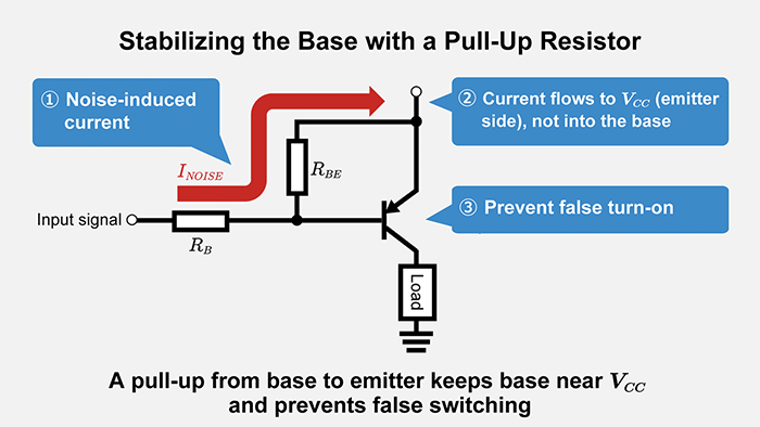
When the microcontroller and load supplies match voltage (e.g., both 5V), raising the microcontroller output to the H level makes the base and emitter equal potential, ensuring reliable turn-off. However, when both supplies differ, attention is required.
For example, with load supply at 12 V and microcontroller supply at 5 V, even raising microcontroller output to H level (5 V) leaves the base at lower potential than the emitter (12 V), keeping the BE junction forward-biased (of the approximately 7 V potential difference, about 0.7 V appears across the base-emitter junction, and the remainder drops across the base resistor). In this state, the transistor remains on. Furthermore, current from the 12 V system flows into the 5 V system microcontroller pin through the base resistor, exceeding the microcontroller’s supply voltage and causing injection current / back-powering through the pin’s protection diodes. Do not allow the base input voltage to exceed the controller’s supply voltage; use an NPN-level shifter when the supplies differ. To ensure reliable turn-off while protecting the microcontroller, a level-shift circuit using an NPN transistor is essential.
Wiring and Protection Techniques for Safe, Stable Operation
In inductive-load drive circuits, back-EMF during switch-off can destroy transistors. When switching off circuits that drive loads such as relays or motors, back-EMF is generated. When this voltage exceeds the transistor’s breakdown voltage ratings, device failure occurs. Placing a flyback (freewheel) diode in parallel with the load absorbs back-EMF and protects the transistor. For high-side configurations, correct diode placement relative to +V is essential. Floating-base conditions cause malfunctions, requiring pull-up resistors for stability.
Diode Placement Method to Protect Inductive Loads
In circuits driving inductive loads (relays, motors, solenoids), back-EMF is generated the instant the transistor switches off. When this voltage exceeds the transistor ratings, the transistor may enter breakdown (avalanche) and can be damaged.
In a high-side PNP switch (emitter at +V, load to GND), the flyback diode should be placed in parallel with the inductive load. Connect the cathode to the collector node (the load’s high side when ON) and the anode to GND.
When the transistor turns off, the inductor current cannot stop instantly. The load’s top node (collector node) is driven below 0 V, forward-biasing the diode. Current then recirculates in the loop GND → diode → load → GND, clamping the node near approximately − VF and preventing excessive voltage stress on the transistor. This diode protects the transistor from back-EMF by providing a controlled current path and limiting the transient | VCE| to a safe range (verify the device’s breakdown ratings in the datasheet).
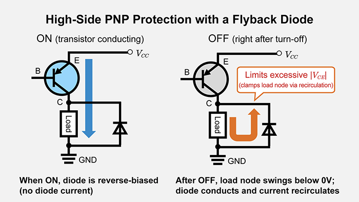
While diodes suppress back-EMF voltage, they slow current decay, slightly delaying relay release. For fast-cutoff requirements, consider a series Zener diode or an RC snubber. Circuits without diodes risk destruction during initial switching, depending on the magnitude of back-EMF relative to the device’s breakdown voltage ratings.
Preventing Malfunction Through Base Handling and Wiring (Floating and Potential Differences)
Base floating prevention can be addressed with the pull-up resistors covered in the previous section. This section covers wiring, routing, and noise countermeasures.
Long wiring from the emitter to the supply (+V) makes circuits more susceptible to noise and can cause malfunctions. Connecting the emitter terminal to board supply lines via the shortest paths improves noise immunity. When supply line impedance is high, placing bypass capacitors (0.1 μF–1 μF guideline) near the emitter suppresses high-frequency noise.
Base wiring similarly benefits from shorter paths from the microcontroller output to the base resistor, reducing noise susceptibility. Long base wiring allows external noise to disturb base potential, potentially causing transistors to turn on at unintended times.
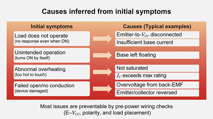
Common High-Side Drive Problems and Solutions
The three most frequent high-side switch problems are no operation due to wiring errors, dim lighting when off, and damage from reverse connection. When loads don’t operate, verify the emitter connection to +V and that the base voltage is sufficiently lower than the emitter. When loads don’t fully turn off and remain dimly lit, either the base is floating, or the emitter-to-base potential difference is insufficient. Executing minimum wiring checks enables rapid fault isolation.
Incomplete Turn-Off / Dim Load Lighting Causes
The “load doesn’t turn off completely and stays dimly lit” problem in high-side switches stems from multiple overlapping causes. The most common are base-floating and voltage-difference issues with microcontroller supplies.
When the base floats, noise makes the base potential undefined and transistors partially turn on. This occurs when pull-up resistors aren’t used or when the resistance values are too high. When the microcontroller and load supply voltages differ, even raising the microcontroller output to the H level leaves the base at a lower potential than the emitter, keeping the BE junction forward-biased (the junction clamps at approximately 0.7 V, with the remaining voltage dropping across the base resistor). In this state, transistors cannot fully turn off.
A temperature rise increases leakage currents (ICEO and ICEX), leading to weak current flow even when off. If the load stays dimly lit, check leakage currents (ICEO) and base floating. Verify temperature characteristics in the datasheets to confirm that leakage currents remain within acceptable ranges across the operating temperature range. For LED loads, even tens of microamperes can produce visible brightness.
Symptoms and Countermeasures for Reverse Connection and Wiring Errors
High-side wiring faults can be narrowed down from symptoms. When loads don’t operate at all, either the emitter-to-+V connection is broken, or the base voltage isn’t sufficiently lower than the emitter. When loads operate at unintended times, the base terminal is floating.
When transistors overheat, either saturation conditions aren’t met, or the collector current exceeds the maximum rating. Cutoff behaves as high resistance; saturation behaves as low resistance across C–E. When transistors fail and stop conducting, either back-EMF overvoltage or emitter-collector reverse connection is the cause.
Checking wiring before power-on prevents transistor damage and malfunction. Follow these three steps to ensure safety:
- Verify continuity between emitter and +V
- Verify base resistor and load polarity (emitter to +V, collector to ground through load)
- Verify load position (load is on the collector side, between the collector and the ground)
This sequence reveals most wiring errors before power-on.
Summary
When using PNP transistors (bipolar junction transistors) as high-side switches in switching applications, design success depends on three elements. First, place the emitter on the supply side (+V) and the collector on the load side. Second, understand that saturation mode provides low resistance for efficient switching. In contrast, active mode provides current gain. Still, it is unsuitable for switching—pull the base voltage below the emitter voltage to turn “on,” and raise the base voltage reliably to the emitter voltage to turn “off.” Remember: saturation mode for switching efficiency, active mode for current gain in amplification, and correct base handling for reliable turn-off. Third, for inductive loads like relays, place flyback diodes correctly relative to +V to prevent breakdown-voltage violations and prevent unintended on states through proper base handling in the PNP transistor circuit. Historically, germanium transistors were standard; modern high-side switching uses silicon BJTs. PNP devices also appear in complementary push-pull stages of class B amplifiers; detailed design is outside this scope.
Related article
Bipolar Junction Transistor (BJT) Basics: Operation and Applications (NPN & PNP)
NPN Transistor: Low-Side Switch Fundamentals
【Download Documents】 Basics of Si Power Devices
In this handbook, although there are so many types of power devices using Si semiconductors, the basic points are explained, focusing mainly on diodes and transistors for power supply applications. It also introduces the procedure and decision method for transistor selection when designing circuits, as well as application examples that utilize each characteristic and feature.

Transistors
Basic
-
Basics of Transistors
- Transistor Fundamentals: Structure, Types, and Operating Principles
- Bipolar Junction Transistor (BJT) Basics: Operation and Applications (NPN & PNP)
- NPN Transistor: Low-Side Switch Fundamentals
- PNP Transistor: High-Side Switch Fundamentals
- MOSFET Basics: Parasitic Capacitance, Gate Charge, Miller Region, and Threshold Voltage
- MOSFET On-Resistance (RDS(on))
- Super junction MOSFET (SJ MOSFET) Basics
- What is a Digital Transistor?
- Digital Transistor Selection
- How to select<Selecting Transistors to Ensure Safe Operation>
- Junction Temperature <Calculating Transistor Chip Temperature>
- What is a Load Switch?
- Basics of MOSFETs
- Introduction
-
Confirming the Suitability of a Transistor in Actual Operation – Introduction
- Confirmation of the Chip Temperature
- Confirmation of Suitability in Actual Operation and Preparations
- Confirmation that Absolute Maximum Ratings are Satisfied
- Confirmation that Operation is within the SOA (Safe Operating Area)
- Confirmation that Operation is within the SOA Derated at the Actual Operating Temperature
- Confirmation that Average Power Consumption is within the Rated Power
- Summary
- Summary
Evaluation
-
The Importance of the Recovery Characteristics of Primary-side Switching Elements in LLC Converters -Introduction-
- Basic Configuration of an LLC Converter
- Features of LLC Converter Operation
- Basic Operation of LLC Converters
- Importance of MOSFET Recovery Characteristics for Off-Resonance of LLC Converters
- The Importance of the Recovery Characteristics of Primary-side Switching Elements in LLC Converters ーSummaryー
-
The Importance of the Reverse Recovery Characteristics of Switching Elements in Inverter Circuits -Introduction-
- Types of Inverter Circuits and Energization Methods
- Basic Operation of 3-Phase Modulation Inverter Circuits
- Comparison of Losses in a PrestoMOS™ MOSFET and a Standard SJ MOSFET Using Double-Pulse Tests (Actual Measurement Results)
- Comparison of Efficiency of a PrestoMOS™ MOSFET and a Standard SJ MOSFET in a 3-Phase Modulation Inverter Circuit (Simulations)
- The Importance of the Reverse Recovery Characteristics of Switching Elements in Inverter Circuits -Summary-
- Mechanisms of MOSFET Destruction
- About Double-Pulse Tests
-
Improving the Power Conversion Efficiency of Phase Shift Full Bridge Circuits – Introduction
- Basic Configuration of a PSFB Circuit
- Basic Operation of PSFB Circuits
- Guidelines Relating to Operation of Switching Elements Under Light Loading
- Guidelines Relating to Operation of Switching Elements Under Heavy Loading
- Evaluation of Efficiency
- Improving the Power Conversion Efficiency of Phase Shift Full Bridge Circuit – Summary –