Transistors|Basic
MOSFET On-Resistance (RDS(on))
2026.06.15
table of contents
- ・Relationship Between MOSFET On-Resistance and Conduction Loss
- ・Electrical Characteristics of On-Resistance (RDS(on))
- ・Practical Conduction Loss Calculation (Considering Duty and Temperature)
- ・Do Not Choose by On-Resistance Alone: Trade-off Between Conduction Loss and Switching Loss
- ・On-Resistance Comparison by Package
RDS(on) is the drain-to-source on-resistance of a MOSFET in the on-state, and it is a critical parameter because it directly affects conduction loss and heat generation. RDS(on) varies with operating conditions such as gate-to-source voltage (VGS) and junction temperature (TJ): it generally increases as temperature rises or as VGS decreases. In high-current applications such as power supplies and motor drives, even small differences in RDS(on) translate into significant differences in loss and temperature rise, so it is important to understand how to read datasheet conditions and estimate losses with an adequate design margin. This article explains how to interpret RDS(on) specifications, how to calculate conduction loss, and what to consider when selecting a MOSFET for your application.
Relationship Between MOSFET On-Resistance and Conduction Loss
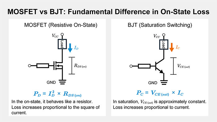
MOSFET on-resistance RDS(on) is the basis for estimating on-state (conduction) loss. For comparison, when a bipolar junction transistor (BJT) is used as a saturated switch, the on-state loss is mainly determined by the collector-emitter saturation voltage VCE(sat). A MOSFET, on the other hand, behaves like a resistor in the on-state, so the conduction loss increases in proportion to the square of the current. The following summarizes the difference in how on-state loss is expressed.
Difference in How Loss Is Expressed for MOSFETs and BJTs
When a BJT operates as a switch in saturation, the on-state conduction loss is:
\(P_C=V_{CE(sat)} ×I_C\)
where PC is the collector power loss, VCE(sat) is the collector-emitter saturation voltage, and IC is the collector current.
For a MOSFET, the drain-to-source path behaves resistively in the on-state so that conduction loss can be approximated as:
\(P_D≈I_D^2×R_{DS(on)}\)
where PD is the MOSFET power dissipation due to conduction, RDS(on) is the drain-to-source on-resistance, and ID is the drain current.
This loss appears as heat inside the MOSFET and is dissipated through the package and the PCB. Therefore, a lower RDS(on) reduces conduction loss and simplifies thermal design. Note, however, that the actual temperature rise depends not only on RDS(on) but also on junction temperature, PCB layout, thermal environment, and switching conditions.
Electrical Characteristics of On-Resistance (RDS(on))
Always Consider the Test Conditions (VGS / ID / TJ)
RDS(on) is not a single fixed value. It depends on operating and measurement conditions such as gate-to-source voltage (VGS), drain current (ID), and junction temperature (TJ). Because datasheet RDS(on) values are always specified together with these conditions, device-to-device comparison should be performed using the same conditions, and design calculations should include a margin for your actual operating environment.
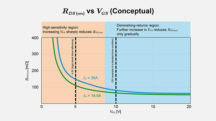
Variation with VGS and ID: Selecting RDS(on) for Loss Calculations
As shown in typical characteristic curves, RDS(on) decreases as VGS increases. In addition, even at the same VGS, the effective RDS(on) can vary with ID (especially at high current due to self-heating). When calculating loss, use an RDS(on) value (or curve) corresponding to the gate drive voltage you will actually apply (for example, 4.5 V, 5 V, or 10 V) and the current level relevant to your application. If the datasheet lists multiple RDS(on) values at different VGS, use the condition closest to your actual gate drive as the reference.
Estimating RDS(on) in the Ohmic Region and Relating It to Conduction Loss
When a MOSFET is fully enhanced, and the drain-to-source voltage VDS is relatively small (the resistive/ohmic region), RDS(on) can be approximated from the operating point as:
\(R_{DS(on)} ≈ \displaystyle\frac{V_{DS}}{I_D} \)
Using this approximation, conduction loss can be estimated by:
\(P_D ≈ I^2×R_{DS(on)} \)
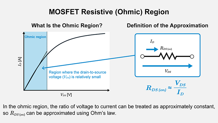
If the current is not constant, use the RMS current IRMS for the relevant on-interval.
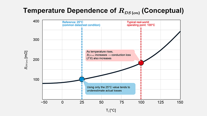
RDS(on) Increases as Temperature Rises
RDS(on) also varies with temperature. In general, it has a positive temperature coefficient, meaning RDS(on) increases as the junction temperature rises. Because the datasheet RDS(on) is often specified at TJ = 25 °C, loss calculations for real operating conditions should account for the increase in RDS(on) at elevated temperature.
Datasheet Values (typ/max) and How to Set Design Margin
Datasheets may list RDS(on) as both a typical value (typ) and a maximum guaranteed value (max). When designing for loss and temperature rise, it is generally safest to base calculations on the max value, and then apply the temperature dependence (from the RDS(on) vs. temperature characteristics) to reflect the expected TJ. Typical values are useful to understand what performance is common, but using typ for worst-case loss estimation is risky because it ignores production spread and high-temperature degradation.
Practical Conduction Loss Calculation (Considering Duty and Temperature)
Basic Formula: Conduction Loss Is I2 × RDS(on)
The fundamental relationship for MOSFET conduction loss is the I²R loss of the on-resistance:
\(P_D =I^2×R_{DS(on)} \)
Here, I is the current through the MOSFET during the on-state.
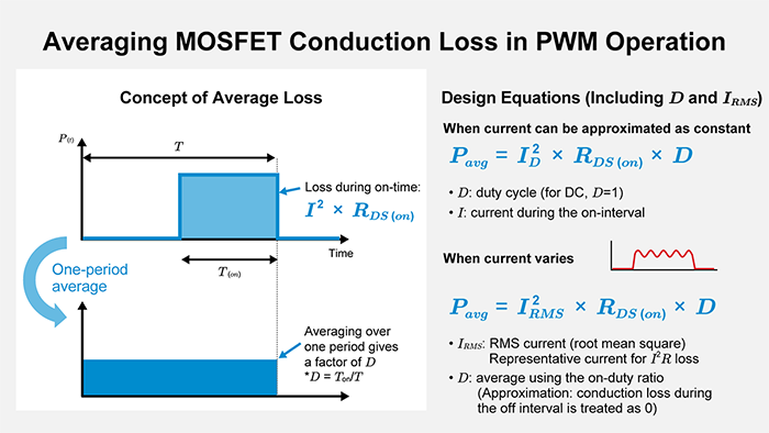
Include Duty Cycle and RMS Current (IRMS) to Obtain Average Loss
In real circuits, the MOSFET is not continuously on, and the current is not always constant. For PWM drive or intermittent operation, include the duty cycle D (fraction of time the MOSFET is on). The average conduction loss can be estimated as:
\(P_{avg} =I^2×R_{DS(on)} ×D\)
For DC conduction, D = 1.0. If current varies, replace I with the RMS current during the on-interval:
\(P_{avg} =I_{RMS}^2×R_{DS(on)} ×D\)
Correct for Temperature Rise Using a Temperature Multiplier k
In actual operation, self-heating increases TJ and, consequently, RDS(on) compared with the datasheet value measured at 25 °C. A practical way to include this effect is to use a temperature multiplier k obtained from the datasheet RDS(on) vs. temperature characteristic:
\(P_{avg(actual)}\ =I_{RMS}^2×R_{DS(on)} ×D×k\)
where k = RDS(on) at the operating junction temperature divided by RDS(on) at 25 °C. For example, if RDS(on) is 10 mΩ at 25 °C and 15 mΩ at 100 °C:
\(k=\displaystyle\frac{15mΩ}{10mΩ}\ =1.5\)
In practical design, calculate conduction loss by properly accounting for both the duty cycle and the temperature multiplier.
Include Mounting Resistance and Self-Heating (Thermal Resistance) in the Estimate
When RDS(on) is in the milliohm range, resistances in series with the MOSFET can also matter. PCB copper traces, vias, connectors, and other interconnects add series resistance, so the circuit’s effective conduction loss is often better estimated using an equivalent resistance:
\(P_{avg} =I_{RMS}^2×(R_{DS(on)} +R_{wiring})×D\)
To choose an appropriate temperature multiplier k, you first need an estimate of the operating junction temperature TJ. A simple first-order estimate is based on ambient temperature TA and junction-to-ambient thermal resistance RθJA: TJ ≈ TA + Ptotal × RθJA. If case temperature TC is known, you can instead use junction-to-case thermal resistance RθJC: TJ ≈ TC + Ptotal × RθJC. Here, Ptotal is the total device loss, including both conduction loss and switching loss.
A practical workflow is:
- First, calculate conduction loss using the datasheet RDS(on) near 25 °C, and add switching loss if necessary to obtain an initial Ptotal.
- Next, estimate TJ from Ptotal and the appropriate thermal resistance (for example, RθJA).
- Finally, update RDS(on) using the temperature characteristic (i.e., update k for that TJ) and, if needed, recalculate Ptotal once more.
Even a single pass of this “loss → temperature → RDS(on)” consistency check helps you set a more realistic design margin for temperature rise.
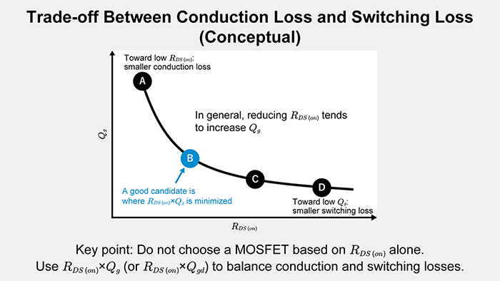
Do Not Choose by On-Resistance Alone: Trade-off Between Conduction Loss and Switching Loss
Lower RDS(on) Often Increases Qg and Parasitic Capacitances
Reducing RDS(on) lowers conduction loss (I2R), but switching-related losses may become dominant in some applications. In many cases, achieving a lower RDS(on) requires a larger silicon die area. A larger die tends to increase gate charge Qg and parasitic capacitances, thereby increasing switching and gate-drive losses. Therefore, the device with the lowest RDS(on) is not always the device with the lowest total loss, especially at higher switching frequencies.
Balance Using RDS(on)×Qg (or RDS(on)×Qgd)
For switching power converters and other high-frequency applications, it is useful to evaluate a balance metric such as RDS(on)×Qg (or RDS(on)×Qgd). This type of figure of merit helps compare the trade-off between conduction loss (driven by RDS(on)) and switching/gate-drive loss (related to charge and capacitance). It makes it easier to select a MOSFET that minimizes total loss in the intended operating region.
On-Resistance Comparison by Package
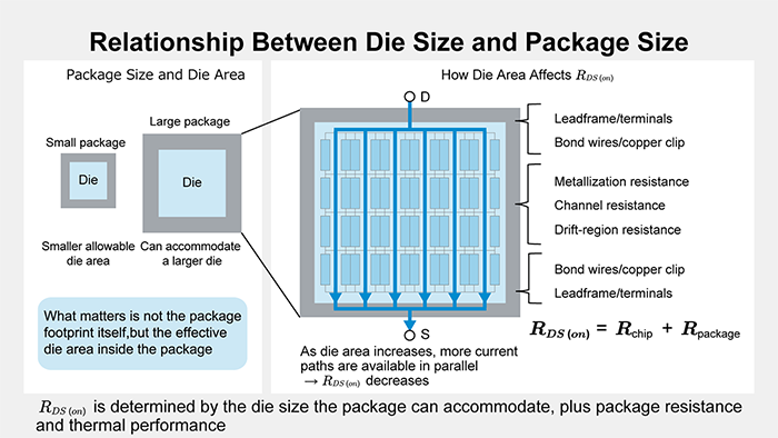
Relationship Between Chip Size (Die Area) and Package Size
It is often said that “a larger package has lower on-resistance,” but the key factor is not the package surface area itself. The dominant factor is the maximum silicon die area that can be mounted in that package. Power MOSFETs have many cells in parallel, so a larger die area provides more parallel current paths and tends to reduce RDS(on). In addition, the RDS(on) specified in a datasheet is not only the intrinsic silicon resistance; it is the total resistance along the current path from the drain to the source. This includes contributions from channel resistance, drift-region resistance, metallization resistance, and package-related resistances (for example, leadframe, bond wires, copper clip, and terminal/pad resistance). Therefore, changing the package can change both the die size limit and the package’s own resistance and thermal behavior, all of which affect the measured RDS(on).
For High Current, Terminal Structure/Layout (Kelvin Source) Matters
In the milliohm range, high-current switching and parasitic inductance in the PCB and package (common-source inductance) can cause source voltage bounce. This effectively reduces the gate-to-source voltage seen by the channel, potentially degrading conduction behavior. To mitigate this, Kelvin-source packages that separate the power source terminal from the gate-drive reference source can be effective, as can PCB layouts that keep the gate-return (source) path separate from the power current loop. In practice, evaluating terminal structure and layout robustness, along with the RDS(on) number, helps reduce performance variation after assembly.
Related article
Transistor Fundamentals: Structure, Types, and Operating Principles
MOSFET Basics: Parasitic Capacitance, Gate Charge, Miller Region, and Threshold Voltage
【Download Documents】 Basics of Si Power Devices
In this handbook, although there are so many types of power devices using Si semiconductors, the basic points are explained, focusing mainly on diodes and transistors for power supply applications. It also introduces the procedure and decision method for transistor selection when designing circuits, as well as application examples that utilize each characteristic and feature.

Transistors
Basic
-
Basics of Transistors
- Transistor Fundamentals: Structure, Types, and Operating Principles
- Bipolar Junction Transistor (BJT) Basics: Operation and Applications (NPN & PNP)
- NPN Transistor: Low-Side Switch Fundamentals
- PNP Transistor: High-Side Switch Fundamentals
- MOSFET Basics: Parasitic Capacitance, Gate Charge, Miller Region, and Threshold Voltage
- MOSFET On-Resistance (RDS(on))
- Super junction MOSFET (SJ MOSFET) Basics
- What is a Digital Transistor?
- Digital Transistor Selection
- How to select<Selecting Transistors to Ensure Safe Operation>
- Junction Temperature <Calculating Transistor Chip Temperature>
- What is a Load Switch?
- Basics of MOSFETs
- Introduction
-
Confirming the Suitability of a Transistor in Actual Operation – Introduction
- Confirmation of the Chip Temperature
- Confirmation of Suitability in Actual Operation and Preparations
- Confirmation that Absolute Maximum Ratings are Satisfied
- Confirmation that Operation is within the SOA (Safe Operating Area)
- Confirmation that Operation is within the SOA Derated at the Actual Operating Temperature
- Confirmation that Average Power Consumption is within the Rated Power
- Summary
- Summary
Evaluation
-
The Importance of the Recovery Characteristics of Primary-side Switching Elements in LLC Converters -Introduction-
- Basic Configuration of an LLC Converter
- Features of LLC Converter Operation
- Basic Operation of LLC Converters
- Importance of MOSFET Recovery Characteristics for Off-Resonance of LLC Converters
- The Importance of the Recovery Characteristics of Primary-side Switching Elements in LLC Converters ーSummaryー
-
The Importance of the Reverse Recovery Characteristics of Switching Elements in Inverter Circuits -Introduction-
- Types of Inverter Circuits and Energization Methods
- Basic Operation of 3-Phase Modulation Inverter Circuits
- Comparison of Losses in a PrestoMOS™ MOSFET and a Standard SJ MOSFET Using Double-Pulse Tests (Actual Measurement Results)
- Comparison of Efficiency of a PrestoMOS™ MOSFET and a Standard SJ MOSFET in a 3-Phase Modulation Inverter Circuit (Simulations)
- The Importance of the Reverse Recovery Characteristics of Switching Elements in Inverter Circuits -Summary-
- Mechanisms of MOSFET Destruction
- About Double-Pulse Tests
-
Improving the Power Conversion Efficiency of Phase Shift Full Bridge Circuits – Introduction
- Basic Configuration of a PSFB Circuit
- Basic Operation of PSFB Circuits
- Guidelines Relating to Operation of Switching Elements Under Light Loading
- Guidelines Relating to Operation of Switching Elements Under Heavy Loading
- Evaluation of Efficiency
- Improving the Power Conversion Efficiency of Phase Shift Full Bridge Circuit – Summary –