Transistors|Evaluation
Basic Configuration of a PSFB Circuit
2021.09.15
Points of this article
・Phase shift full bridge (PSFB) circuits make possible dramatic reductions in switching losses through zero-voltage switching (ZVS) operation of switching elements, and so can handle greater amounts of power.
・A PSFB switching circuit essentially consists of four switching elements (MOSFETs); the leakage inductance of a transformer is used as a resonance inductance necessary for ZVS operation.
・In order to extend the range of ZVS operation, there are cases in which an inductor is added in series. Here, a circuit with an added series inductor is assumed.
・In the basic switching operation, after the on/off states of Q1 and Q2 have been swapped, the on/off states of Q3 and Q4 are swapped after a certain phase lag.
・In general, the leg of Q1 and Q2 is called the "leading leg", and the leg of Q3 and Q4 is the "lagging leg".
Basic Configuration of a PSFB Circuit
To begin with, the basic configuration of a PSFB circuit is presented. Upon grasping this basic configuration, the circuit operation, described below, should also be easy to understand.
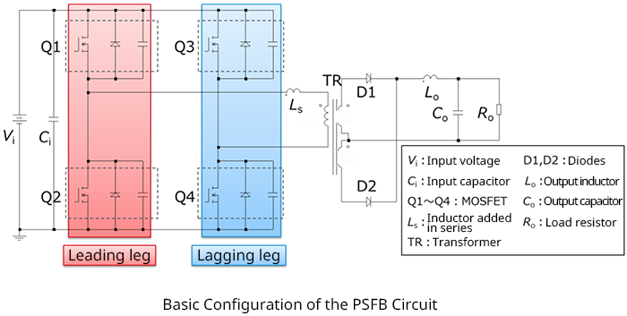
The leakage inductance of the transformer may be utilized as a resonance inductor in order to realize ZVS, which is one feature of the PSFB configuration; however, in some cases an inductor is added in series with the transformer to broaden the range of ZVS operation. Here, a circuit is assumed in which an added series inductor LS is used.
Next, the on/off timing chart for the switches is shown. The figures appearing in the bottom below the bidirectional arrows are labels representing the circuit operation modes. These correspond to the mode numbers used in the following explanation of circuit operation.
As shown in the chart, after the on/off states of Q1 and Q2 have been swapped, the on/off states of Q3 and Q4 are swapped with a certain phase lag. From this fact, the leg of Q1 and Q2 is generally called the “leading leg”, and the leg of Q3 and Q4 is the “lagging leg”.

Transistors
Basic
-
Basics of Transistors
- Transistor Fundamentals: Structure, Types, and Operating Principles
- Bipolar Junction Transistor (BJT) Basics: Operation and Applications (NPN & PNP)
- NPN Transistor: Low-Side Switch Fundamentals
- PNP Transistor: High-Side Switch Fundamentals
- MOSFET Basics: Parasitic Capacitance, Gate Charge, Miller Region, and Threshold Voltage
- MOSFET On-Resistance (RDS(on))
- Super junction MOSFET (SJ MOSFET) Basics
- What is a Digital Transistor?
- Digital Transistor Selection
- How to select<Selecting Transistors to Ensure Safe Operation>
- Junction Temperature <Calculating Transistor Chip Temperature>
- What is a Load Switch?
- Basics of MOSFETs
- Introduction
-
Confirming the Suitability of a Transistor in Actual Operation – Introduction
- Confirmation of the Chip Temperature
- Confirmation of Suitability in Actual Operation and Preparations
- Confirmation that Absolute Maximum Ratings are Satisfied
- Confirmation that Operation is within the SOA (Safe Operating Area)
- Confirmation that Operation is within the SOA Derated at the Actual Operating Temperature
- Confirmation that Average Power Consumption is within the Rated Power
- Summary
- Summary
Evaluation
-
The Importance of the Recovery Characteristics of Primary-side Switching Elements in LLC Converters -Introduction-
- Basic Configuration of an LLC Converter
- Features of LLC Converter Operation
- Basic Operation of LLC Converters
- Importance of MOSFET Recovery Characteristics for Off-Resonance of LLC Converters
- The Importance of the Recovery Characteristics of Primary-side Switching Elements in LLC Converters ーSummaryー
-
The Importance of the Reverse Recovery Characteristics of Switching Elements in Inverter Circuits -Introduction-
- Types of Inverter Circuits and Energization Methods
- Basic Operation of 3-Phase Modulation Inverter Circuits
- Comparison of Losses in a PrestoMOS™ MOSFET and a Standard SJ MOSFET Using Double-Pulse Tests (Actual Measurement Results)
- Comparison of Efficiency of a PrestoMOS™ MOSFET and a Standard SJ MOSFET in a 3-Phase Modulation Inverter Circuit (Simulations)
- The Importance of the Reverse Recovery Characteristics of Switching Elements in Inverter Circuits -Summary-
- Mechanisms of MOSFET Destruction
- About Double-Pulse Tests
-
Improving the Power Conversion Efficiency of Phase Shift Full Bridge Circuits – Introduction
- Basic Configuration of a PSFB Circuit
- Basic Operation of PSFB Circuits
- Guidelines Relating to Operation of Switching Elements Under Light Loading
- Guidelines Relating to Operation of Switching Elements Under Heavy Loading
- Evaluation of Efficiency
- Improving the Power Conversion Efficiency of Phase Shift Full Bridge Circuit – Summary –