
Transistors|Basic
Low-Side Switch Design: NPN Transistor Circuit Design
2026.07.30
table of contents
- ・NPN Low-Side Switch Circuit Configuration
- ・NPN Transistor (Bipolar Transistor) Switching Design Flow
- ・How to Choose Base Resistor RB (NPN Transistor Base Drive)
- ・Design Points for Reliable NPN Transistor Saturation
- ・Protection Circuits for Inductive Loads: Relays and Solenoids
- ・Simple Power Loss and Heating Estimation for Switch Circuits
- ・Minimum Verification Procedures for Actual Hardware Confirmation
- ・Branch Decisions for Higher Current and Efficiency Requirements
- ・Summary (Design Procedure Review and Next Steps)
A low-side switch uses an NPN transistor to control current between a load and ground. This simple circuit configuration drives relays, motors, and other loads from microcontroller GPIO signals in industrial applications and automotive systems. Two design decisions determine circuit performance: the base resistor value for transistor saturation and the diode placement for back-EMF protection. The complete design sequence covers specification definition, component selection, resistance calculation, protection circuits, and operational verification. For fundamentals of NPN transistor operation, refer to “NPN Transistor Basics | Low-Side Switch Fundamentals.” For comprehensive bipolar transistor principles, see “Bipolar Transistors (BJT) | NPN/PNP Fundamentals and Applications.”
NPN Low-Side Switch Circuit Configuration
The overall circuit structure shows how current flows from the power supply through the load to the transistor. Design parameters affect each component position. Examine the complete circuit first to understand component relationships.
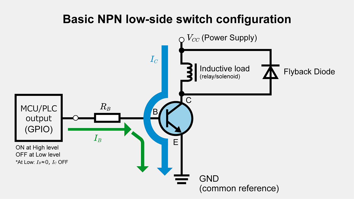
Circuit Overview and Current Flow (Power Supply → Load → NPN → Ground / Diode Position)
Connect the power supply positive terminal to the load, then to the NPN transistor collector, with the emitter connected to the negative side (ground). Current flows as: Power Supply (+V) → Load → Collector → Emitter → Ground. For transistor structure and terminal functions, see “Bipolar Transistors (BJT)“, which explains circuit symbols and terminal definitions.
The microcontroller or PLC output connects to the NPN base through base resistor RB. When the output goes HIGH, the base current IB flows, forward-biasing the base-emitter junction. Collector current IC then flows through the collector-emitter path, energizing the load. When the output goes LOW, the base current drops to near zero, and the transistor turns OFF. Note that the actual HIGH output voltage of a GPIO pin depends on the source current, so that it may be lower than VCC; use the datasheet VOH(min) specification when calculating RB for a conservative design.
Inductive loads, such as relays and solenoids, require a flyback diode. Connect the diode in parallel with the load: cathode facing the power-supply side (+V), Anode facing the transistor side (ground side). When the transistor turns OFF, the coil energy is commutated into the diode loop, limiting the collector-voltage spike across the transistor. Similar considerations apply when switching sensor coils or small motor windings.
Low-Side Switch vs. High-Side Switch Positioning
Transistor-based load switching uses two configurations: low-side and high-side. These two configurations offer different advantages depending on application requirements. Low-side places the switching element on the ground side of the load. High-side places it on the power supply side. Choose a configuration based on safety requirements and measurement needs.
Low-side configuration uses an NPN transistor with a common ground shared between the microcontroller and the load. A single-base resistor enables direct drive from the microcontroller output. Load ground-side floats, requiring careful consideration of current-sensing or protection circuits referenced to ground. Circuit simplicity and component count favor the low-side in cost-sensitive applications.
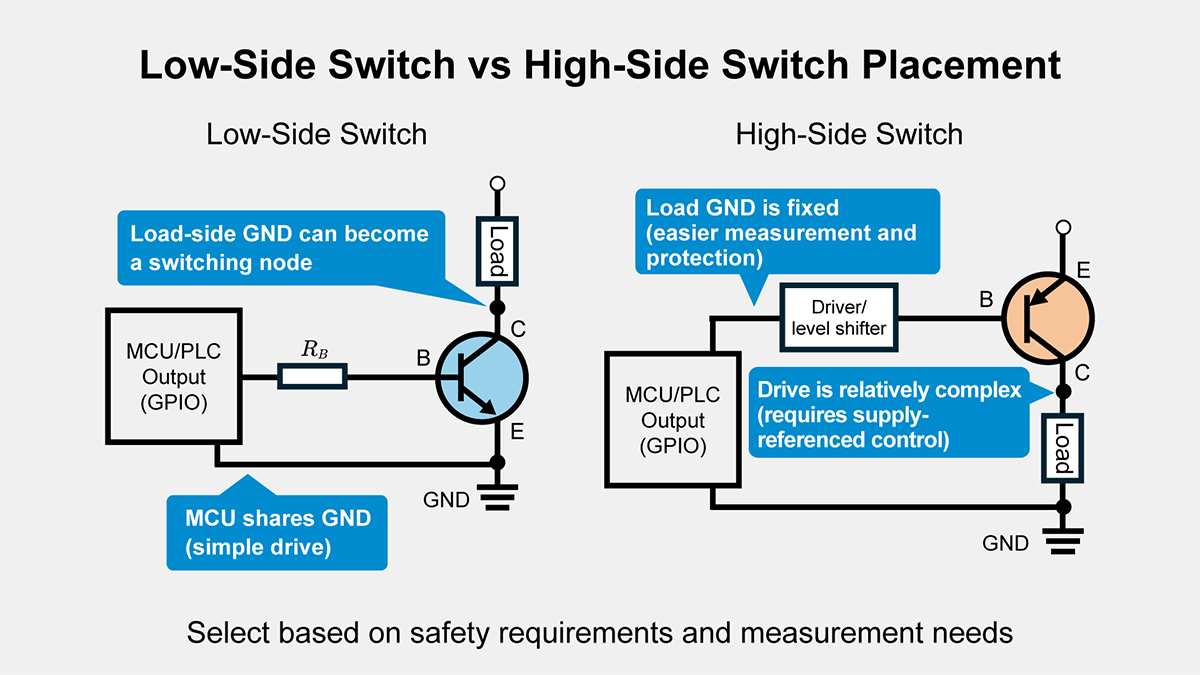
High-side keeps the load permanently grounded, offering safety and measurement advantages. A P-channel MOSFET (P-channel FET) or a PNP transistor is used in a high-side configuration, requiring more complex drive circuits. For high-side basics using PNP transistors, see “PNP Transistor Basics | High-Side Switch Fundamentals.” Microcontroller relay or motor-drive applications prefer low-side operation because current flow is straightforward, fewer components are needed, and circuit schematics are easier to understand.
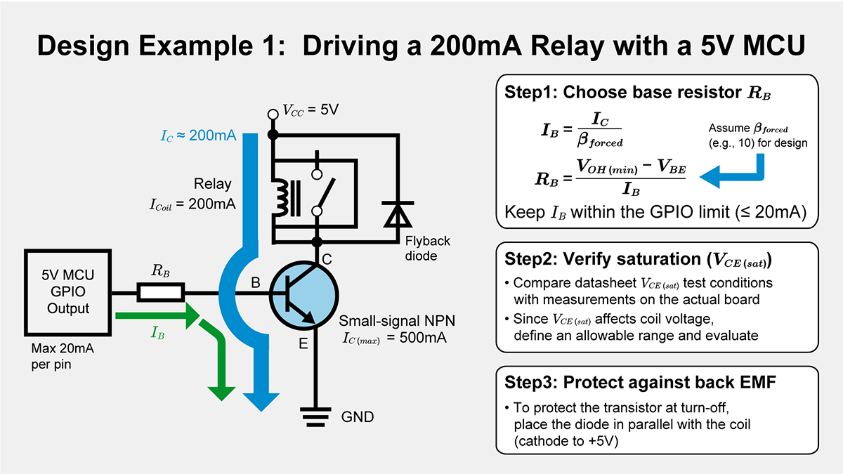
Design Example 1: Driving a 200 mA Relay with a 5 V Microcontroller
A small relay drive from a 5 V microcontroller is a typical application.
| Item | Specification |
|---|---|
| Microcontroller Supply | 5 V |
| GPIO Output | 5 V, 20 mA per port limit |
| Load | 5 V small relay |
| Coil Current | 200 mA |
| Transistor | NPN small-signal (maximum current IC(max) 500 mA class) |
A single microcontroller port drives the relay directly under these conditions. The base resistor is too large, preventing the relay from engaging. The base resistor is too small and exceeds the microcontroller’s current limit. Balance these constraints to achieve reliable switching.
Three decisions define the design. First, determine the base resistor RB value in ohms. Second, confirm the transistor operates in saturation with VCE(sat) within an acceptable range. Third, protect the transistor from coil back EMF. The forced beta value and the GPIO current limit determine the base resistor value. VBE and VCE(sat) datasheet values, when compared with measured values, verify saturation. For detailed power dissipation calculations in transistors, refer to “Component Applied Power Calculation Methods.” Follow the calculation procedures in the subsequent sections.
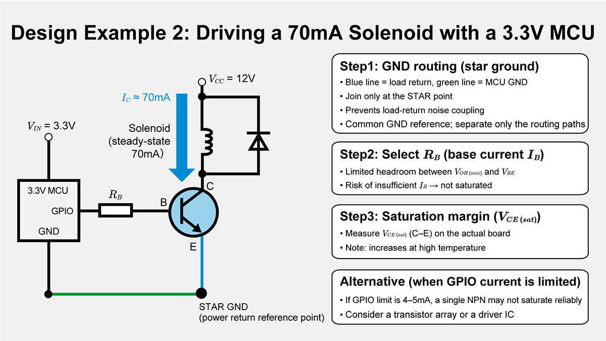
Design Example 2: Driving a 70 mA Solenoid with a 3.3 V Microcontroller
Small solenoid drive from a 3.3 V microcontroller addresses an increasingly common design scenario.
| Item | Specification |
|---|---|
| Microcontroller Supply | 3.3 V |
| GPIO Output | 3.3 V, 12 mA per port limit |
| Load | Small solenoid (rated 12 V) |
| Steady-State Current | 70 mA |
| Power Supply System | 12 V for load, 3.3 V for microcontroller |
| Transistor | NPN small-signal (maximum current IC(max) 200-500 mA class) |
Even if the load supply is 12 V and the microcontroller supply is 3.3 V, a low-side switch still requires a common ground reference: the emitter (GND) must be tied to the microcontroller I/O. Connect the 12 V load ground and the 3.3 V logic ground at a single point (star ground), and keep the high-current return path out of the microcontroller ground wiring.
Lower microcontroller output voltage and lower output current limit create dual constraints compared to 5 V systems. Reliable saturation becomes critical under these conditions. Verify both voltage margin and current capacity before finalizing component selection.
The available voltage for VBE and the base resistor remains limited to 3.3 V. The base current design becomes more stringent. The current limit on IO pins (4-5 mA) makes single-NPN-transistor drive difficult. Switch to transistor arrays or driver ICs under these constraints. For approaches using transistors with built-in base resistors, see “Digital Transistor Selection” for fundamental concepts. Judgment criteria appear with specific examples in the base resistor calculation section.
NPN Transistor (Bipolar Transistor) Switching Design Flow
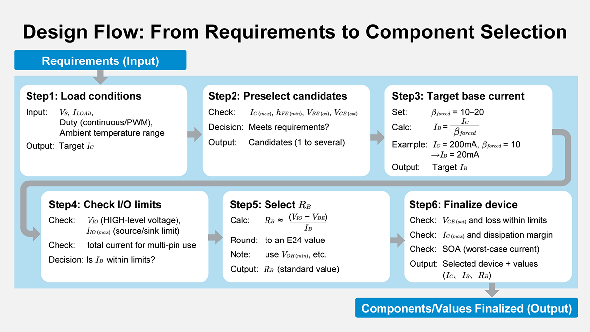
Design begins with a requirements specification: load current, power supply voltage, and GPIO specifications. Follow the sequential flow to determine component selection through resistance values.
Before you start calculating, lock down what you will treat as worst-case (temperature range, supply tolerance, and load variation). A low-side switch looks simple, but the design outcome depends heavily on the worst-case values you assume. Defining those assumptions up front makes later calculations and the prototype evaluation consistent, reducing rework before production.
Flow from Requirements to IC, βforced, IB, and RB
Follow this six-step sequence:
- Define load-side conditions: load voltage VS, load current ILOAD, duty cycle (continuous or PWM), and ambient temperature range. Use these to set the target collector current IC through the transistor (start with IC ≈ ILOAD). If the load is a motor, do not design from steady-state current; use the worst-case startup/stall current. Check not only the continuous IC(max) rating but also the pulse rating and the safe operating area (SOA), and make sure the device cannot be damaged at the peak current.
- Review candidate transistor datasheets: check maximum collector current IC(max), DC current gain hFE(min), typical VBE(on), and VCE(sat), and decide whether the device class meets the requirement.
- Choose a target base current IB using forced current gain βforced: set βforced = 10-20 (do not rely on hFE(min) alone), and calculate IB from βforced = IC / IB (example: IC = 200 mA, βforced = 10 gives IB = 20 mA).
- Check the microcontroller/PLC I/O specifications: verify the HIGH-level output voltage VIO and the source/sink current limits IO(max). Confirm that the required IB fits within the per-pin limit and within any total port/total device current limits when multiple outputs switch simultaneously.
- Calculate the base resistor RB from the available voltage: RB ≈ (VIO – VBE) / RB. Round to a standard resistor value (for example, the E24 series).
- Finalize the component selection: confirm that power dissipation at the designed IC, IB, and VCE(sat) stays within limits with margin, and that IC(max) and maximum power dissipation ratings are not approached under worst-case conditions.
These six steps, in sequence, determine the required components and values from the load conditions. Calculation examples for each step appear in the following sections. Proceed to saturation verification after component finalization.
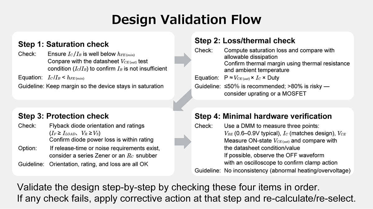
Verification Sequence: Saturation Check → Power Loss Check → Protection → Testing
Verify design validity in this four-step order after determining RB and components:
Saturation Condition Verification
Calculate the IC to IB ratio. Confirm ratio stays sufficiently smaller than hFE(min):
\(\displaystyle\frac{I_C}{I_B} < h_{FE}(min)\)
Compare with the VCE(sat) specification conditions in the datasheet. Check for insufficient IB. A ratio that is too high places the device in the active region, increasing power loss and potentially damaging it. Reduce the ratio by increasing IB or selecting a device with a higher hFE(min).
Power Dissipation and Heating Check
Calculate saturation power loss using VCE(sat), IC, and duty cycle Duty:
\(P≈V_{CE}(sat)\times I_C\times Duty\)
Compare this value with the datasheet’s maximum power dissipation. Below 50% of the maximum power dissipation provides sufficient margin. Above 80% requires a device upgrade or consideration of an MOSFET alternative. Verify thermal resistance and ambient temperature compatibility.
Inductive Load Protection Verification
Verify the flyback diode is correctly oriented: cathode to the power supply side, Anode to the transistor side. Check ratings meet requirements: forward current IF ≥ ILOAD and reverse voltage rating (VR) ≥ VS, with a margin. For release-time or noise requirements, consider adding a series Zener diode or an RC snubber. Confirm diode power dissipation stays within limits.
Minimum Hardware Verification
Measure three parameters with DMM: VBE (0.6-0.9 V range indicates proper bias), IC (consistency with design confirms saturation), VCE(sat) (below 0.3 V in saturation). An oscilloscope is available to observe the turn-off waveform and visually confirm diode clamping action. Record measurements with date, equipment model, and test conditions for documentation.
Check these four items sequentially to systematically verify design validity. Proceed to the base resistor calculation examples in the next section.
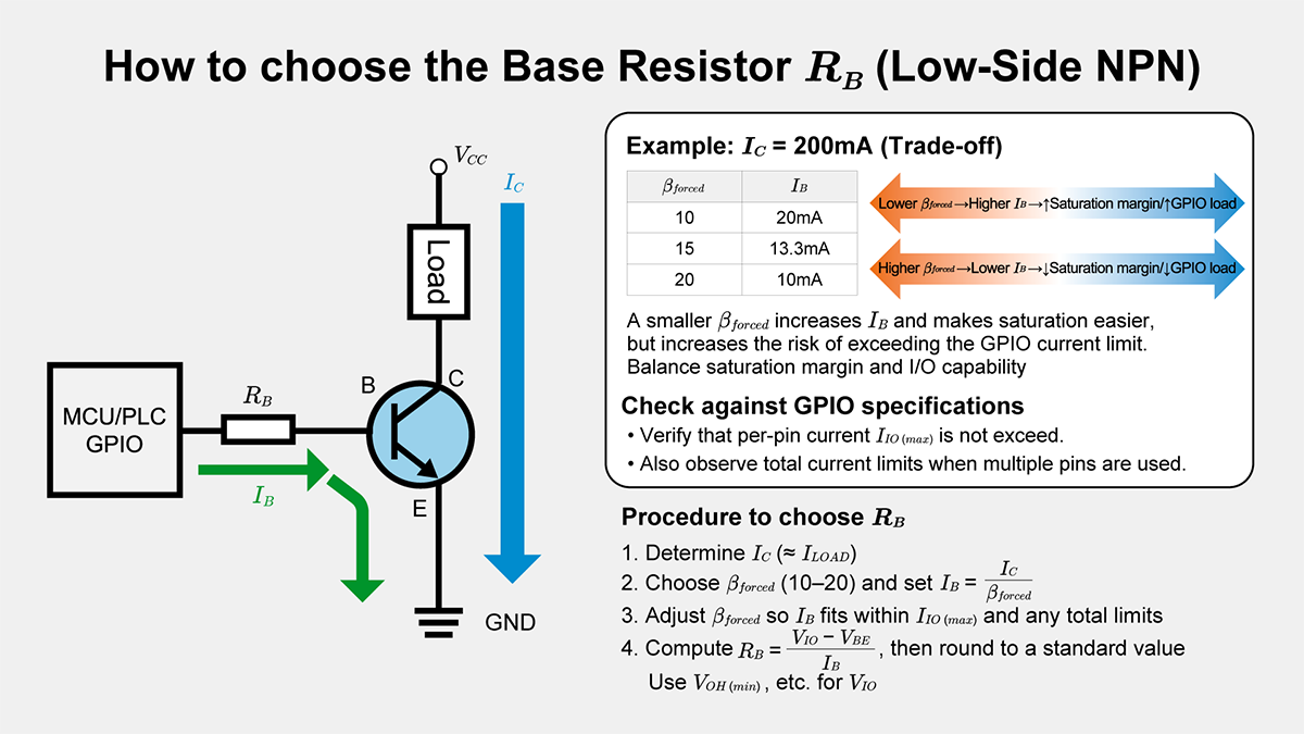
How to Choose Base Resistor RB (NPN Transistor Base Drive)
The base resistor value must satisfy both the transistor’s saturation base current and the GPIO current limits. The calculation formula is straightforward. Forced beta value setting determines design success.
βforced = 10-20 and Comparison with GPIO Current Limits
Datasheet hFE(min) represents the minimum value under specific test conditions. Temperature and individual device characteristics cause variation. Designs relying solely on this value lack a safety margin.
Switch applications intentionally set a small current gain:
\(β_{forced}=\displaystyle\frac{I_C}{I_B}\)
For IC = 200 mA, varying βforced gives:
| βforced | IB |
|---|---|
| 10 | 20 mA |
| 15 | 13.3 mA |
| 20 | 10 mA |
Smaller βforced increases IB, making saturation more reliable. Excessive IB may exceed microcontroller or PLC I/O current limits. Balance reliability against I/O capacity.
Compare the target IB with the microcontroller/PLC specifications after determining IB. Check whether IB the allowable current per I/O pin. Verify total current restrictions during simultaneous multi-pin operation. Example: port limit 20 mA with IB = 20 mA design uses nearly full capacity. Other ports operating simultaneously require verification of the total current restriction. Settle on a realistic value in βforced = 10-20 range while balancing I/O load.
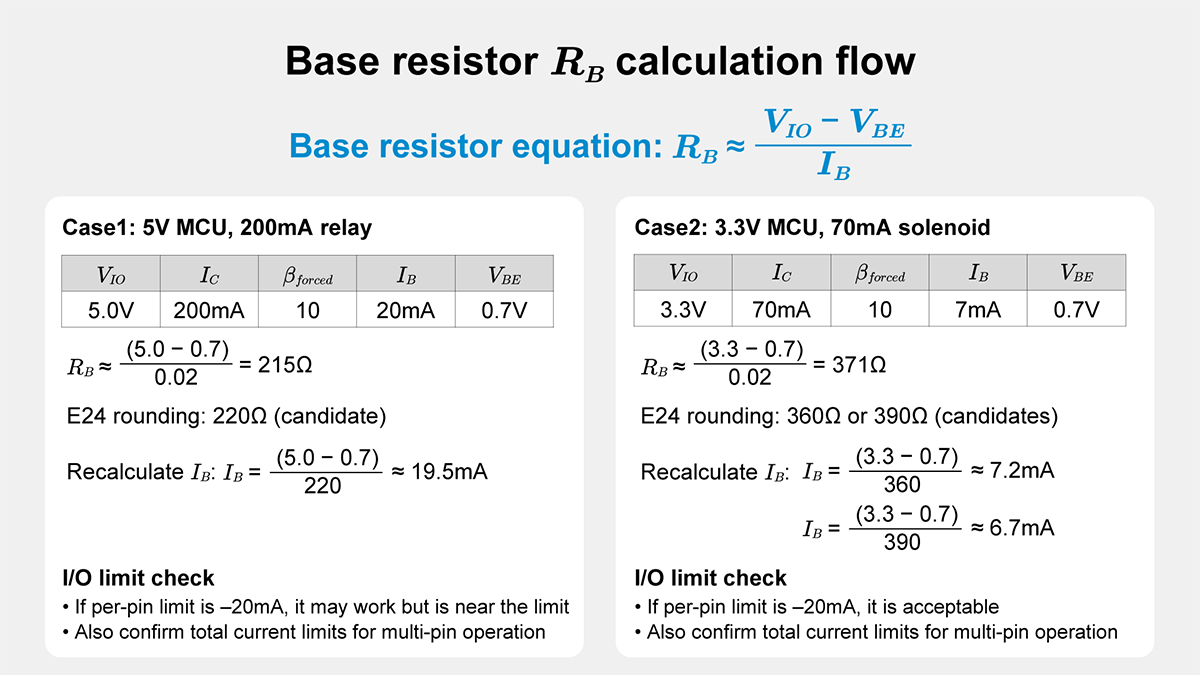
RB Calculation Examples Using 3.3 V/5 V Outputs
Calculate RB after determining IB. Divide voltage difference (I/O output voltage minus VBE) by IB:
\(R_B≈\displaystyle\frac{(V_{IO}−V_{BE})}{I_B}\)
Here, VIO is the actual HIGH-level output voltage of the GPIO pin. It is not always equal to VCC: it drops as the output source current increases. For a conservative design, use the datasheet value VOH(min) at the specified IOH condition rather than assuming the nominal supply voltage. Also treat VBE as a parameter with device and temperature variation (and use VBE(sat) if it is specified). Measure VBE on the first prototype and adjust if needed.
Round calculation results to standard resistor values. Available resistor values are limited to standard series: E12 series (10 % tolerance) or E24 series (5% tolerance). The E24 series provides finer increments (1.0 kΩ, 1.1 kΩ, 1.2 kΩ), making the selection of values close to calculated RB.
Case 1: 5 V Microcontroller Driving 200 mA Relay
Use Design Example 1 conditions:
| Item | Value |
|---|---|
| VIO | 5.0 V |
| IC | 200 mA |
| βforced | 10 |
| IB | 20 mA |
| VBE(on) | 0.7 V |
Calculate RB:
\(R_B≈\displaystyle\frac{(5.0−0.7)}{0.02}=215Ω\)
E24 series closest value: 220 Ω. Recalculate IB with this value:
\(I_B=\displaystyle\frac{(5.0−0.7)}{220}≈19.5 mA \)
This nearly matches the target 20 mA. The I/O pin limit of around 20 mA makes this work. Verify margin, including total current, with other ports. Confirm that no simultaneous high-current port usage exceeds the controller’s total limit.
Case 2: 3.3 V Microcontroller Driving 70 mA Solenoid
Use Design Example 2 conditions:
| Item | Value |
|---|---|
| VIO | 3.3 V |
| IC | 70 mA |
| βforced | 10 |
| IB | 7 mA |
| VBE(on) | 0.7 V |
Calculate RB:
\(R_B≈\displaystyle\frac{(3.3−0.7)}{0.007}=371Ω\)
E24 series candidates: 360 Ω or 390 Ω. Recalculate IB for each:
360 Ω: IB = (3.3 – 0.7) / 360 ≒ 7.2 mA
390 Ω: IB = (3.3 – 0.7) / 390 ≒ 6.7 mA
The I/O pin limit of 8-10 mA means either value provides adequate margin. The 4-5 mA limit makes single-NPN drive difficult. Consider transistor arrays or alternative driver configurations under these constraints.
Also, check the power rating of RB. A quick estimate is PRB ≈ (VIO – VBE)2 / RB (which is the same as IB2 x RB). For Case 1 (VIO = 5.0 V, VBE = 0.7 V, RB = 220 Ω), VIO – VBE = 4.3 V, so PRB ≈ 4.32 / 220 ≈ 0.084 W (about 84 mW). Choosing a 1/8 W (0.125 W) resistor or larger helps maintain thermal margin.
In practice, it is better to choose RB by confirming that the design still works under worst-case conditions, rather than by a one-shot calculation with typical values. The idea is to bound the base current from both sides: on the low-base-current side, make sure IB does not become too small at worst-case low VIO (VOH(smin)), high VBE, and low transistor gain; on the high-base-current side, make sure IB does not exceed the GPIO current limit at worst-case high VIO and low VBE, including resistor tolerance. This two-sided check makes it much easier to explain why the chosen value is robust for production.
Base Series Resistor and Ground Return Wiring Considerations
Circuit placement and wiring require attention after determining RB value. Calculations that are correct but for improper placement or wiring prevent design-as-intended operation.
Place a base series resistor between the I/O pin and the base. No resistance allows unlimited base current, potentially damaging the I/O pin or the transistor. Mistakenly placing resistance on the emitter side raises emitter potential, reducing VBE and preventing adequate transistor turn-on. Verify resistor position before powering the circuit.
Keep emitter-to-ground wiring short. Route base-area wiring to a clean, low-noise ground. Resistance or inductance in the emitter-ground path floats the emitter potential, lowering VBE below design values. High-current handling makes wiring impedance affect VCE, requiring careful attention. Measure actual wiring resistance if currents exceed 500 mA.
A floating base during reset or startup can leave the transistor in an undefined state. Add a bias resistor to define the base potential. In the common case of a push‑pull GPIO driving the base through RB, a pull‑down resistor from base to emitter (ground) keeps the transistor reliably OFF until the microcontroller is initialized. Choose a value on the order of tens of kΩ (much larger than RB), and verify that the pull‑down current is well below your intended base-drive current (for example, < 1% of IB). If you intentionally use open‑drain/open‑collector outputs or inverted logic, choose a pull‑up or pull‑down that sets the safe default state.
Design Points for Reliable NPN Transistor Saturation
Verify the actual VBE and VCE(sat) values against the datasheet specifications to ensure the transistor saturates. Provide margin in the base current. Active-region operation increases power loss and may damage the device.
VBE and VCE(sat) Guidelines and Reading Datasheets
Base resistor calculations assumed VBE(on) = 0.7 V. Actual values vary with device and current but fall within a 0.6-0.8 V range for NPN transistors when on. Assuming approximately 0.7 V in design makes securing margin easier when determining βforced. Measure actual VBE during initial prototype verification.
VCE(sat) is the collector-emitter voltage during saturation. Small-signal transistors under several tens to hundreds of mA conditions typically exhibit values of 0.1-0.3 V. Lower values result in lower switching power loss. Check the datasheet graphs for the variation of VCE(sat) with collector current.
Check datasheet VCE(sat) measurement conditions: specific IC and IB (or IC / IB ratio). Example specification “VCE(sat) = 0.2 V (IC = 100 mA, IB = 10 mA)” represents value at IC / IB = 10 condition.
| Parameter | Typical Value | Verification Point |
|---|---|---|
| VBE(on) | 0.6–0.8 V | Used in RB calculation |
| VCE(sat) | 0.1–0.3 V | Check measurement conditions (IC, IB) |
| IC / IB | 10–20 | Compare with designed βforced |
These three parameters determine the saturation margin. Confirm values before finalizing design.
Verify with a specific example. Datasheet shows “VCE(sat) = 0.2 V (IC = 150 mA, IB = 15 mA)” and design uses IC = 200 mA, IB = 20 mA. Design IC / IB = 10 matches datasheet IC / IB = 10. VCE(sat) is expected to be equal to or slightly higher than the datasheet value under these conditions.
Design using IC = 200 mA and IB = 10 mA yields IC / IB = 20, exceeding the datasheet conditions. VCE(sat) may exceed 0.2 V, indicating insufficient saturation. Review design by increasing IB or reducing βforced. Measure actual VCE during testing to confirm saturation.
Base Current Margin to Avoid Active Region Operation
An insufficient base current causes the transistor to operate in the active region, increasing VCE. Saturation VCE(sat) = 0.2 V can rise above 1 V in the active region. This state increases power loss more than 5-fold, potentially damaging the device through heating. A temperature above 100 °C indicates active-region operation.
Secure sufficient IB to operate in saturation. Switch applications determine IC from load, making IB sufficiently larger. Set intentionally smaller βforced rather than using datasheet hFE(min) directly.
Compare hFE(min) and βforced relationships:
| hFE(min) | βforced | Margin |
|---|---|---|
| Around 100 | 10–20 | 1/5 to 1/10 of hFE |
| Around 50 | 8–10 | 1/5 to 1/6 of hFE |
This setting maintains saturation even when hFE varies with temperature and device characteristics. hFE tends to increase with rising temperature but decreases at low temperatures. A transistor with hFE = 100 at room temperature may drop to hFE = 50 in cold environments or at high collector current. This is particularly important in harsh environments such as automotive and vehicle applications, where temperature variations are significant. Setting βforced = 10-20 provides a margin accounting for such variations.
Making βforced too small increases IB, leading to side effects such as exceeding microcontroller I/O limits or increased base drive loss. βforced = 10-20 represents a balanced range between saturation reliability and I/O load. Alternative approach of making βforced larger (30-50) to reduce IB is not recommended because temperature variation and device tolerance can push operation into the active region, defeating the purpose of margin design.
Compare the designed IC /IB with the datasheet conditions. Confirm the design value stays smaller. Meeting this condition keeps the active region risk low. Test the initial prototype at temperature extremes to verify the adequacy of the margins.
Protection Circuits for Inductive Loads: Relays and Solenoids
Inductive loads generate back EMF when the transistor turns off. The flyback diode provides a current path to protect the device. Fast release requirements use series Zener diodes or RC snubbers.
Flyback Diode Orientation and Current/Voltage Ratings
Coil loads, such as relays and solenoids, generate back EMF the moment the transistor turns off. This voltage is generated when the coil’s stored energy is released and can range from several tens of volts to well over 100 V, depending on the wiring and clamp method. If the transient exceeds the transistor voltage rating, it can destroy the device. Protect the switch with a flyback diode.
Orient the diode with the cathode toward the power supply side (+V) and the Anode toward the transistor side (ground side). This orientation reverses the diode’s bias when the transistor is on, so no current flows through it. The turn-off moment creates a path for the coil current to circulate through the diode, preventing excessive voltage across the transistor. Incorrect orientation, short power supply, or provides no protection. Verify polarity markings before soldering.
Check two ratings for diode selection:
| Rating Item | Selection Criterion | Example |
|---|---|---|
| Forward Current IF | Equal to or greater than coil current ILOAD | ILOAD = 200 mA → IF ≥ 200 mA |
| Reverse Voltage VR | Exceed VS, max with margin (3-5x nominal is a common starting point) | VS = 12 V → VR ≥ 50 V |
Forward current rating must be at least the coil current ILOAD because the coil current commutates into the diode at turn-off. For reverse voltage, the key rating is VR (often specified as VRRM). It must exceed the worst-case load supply voltage VS, max, and it should include a margin for supply surges/spikes and wiring-related transients. A common rule-of-thumb is to pick VR around 3-5x the nominal supply (for example, 12 V -> 50 V or higher), but treat this as a starting point and validate against your system environment.
For most relay/solenoid loads, a general-purpose silicon rectifier diode is sufficient. Schottky diodes have a low forward drop and essentially no reverse recovery, but many parts have relatively low reverse-voltage ratings. Also note that a lower forward drop lowers the clamp voltage, which slows coil current decay and tends to make relay/solenoid release slower. If you need a faster release, use a higher-voltage clamp (for example, a series Zener) or an RC snubber rather than relying on a Schottky swap. For Design Example 1 (5 V, 200 mA), choosing a widely available 1 A-class rectifier diode with adequate reverse-voltage margin (often 50-100 V or higher) is a robust starting point. For Design Example 2 (12 V, 70 mA), a 1 A-class rectifier diode is readily available and provides a comfortable margin; choose VR based on VS, max, and expected transients. In all cases, verify the diode junction temperature stays within its rating during operation.
Series Zener/RC Snubber for Fast Release Requirements
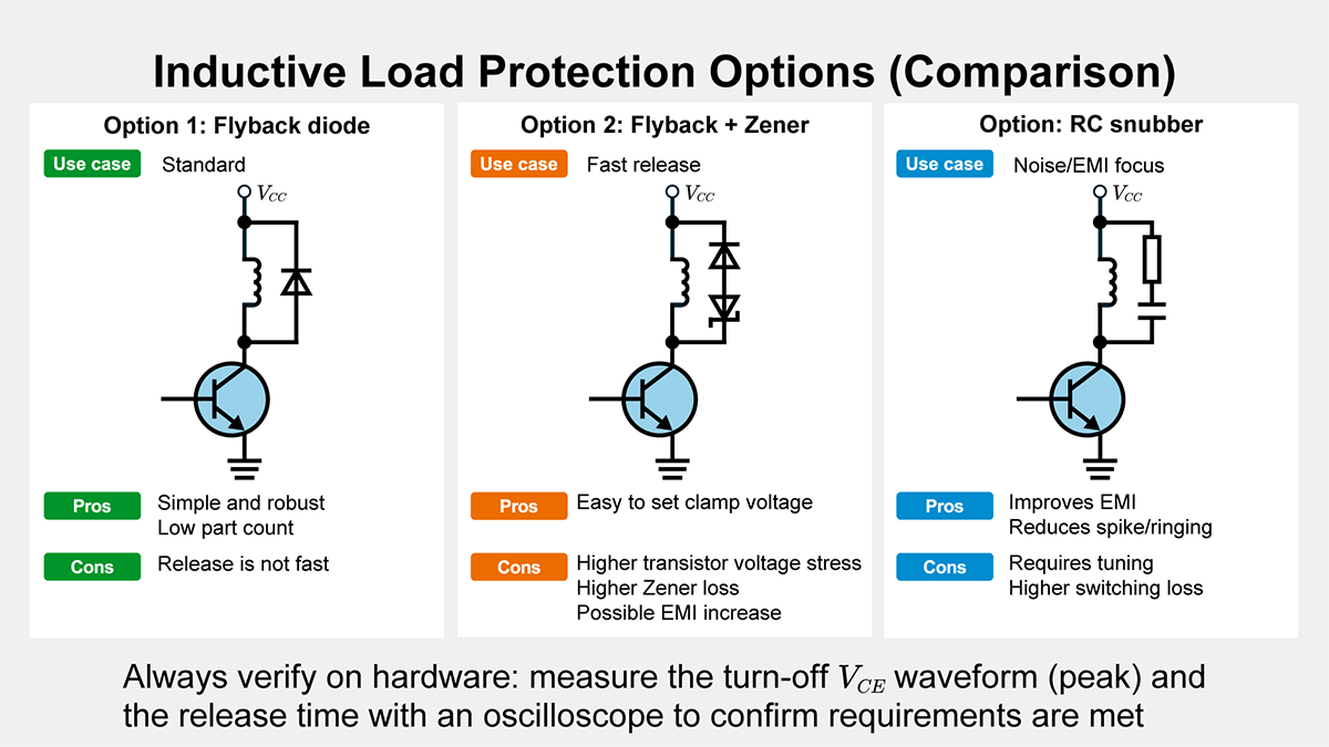
Flyback diodes effectively suppress back EMF but slow coil current decay. Relays show extended release time. Solenoids show lengthened return time. High-speed on/off cycling applications face time constraints on decay time. Speed release with series Zener diodes or RC snubbers.
Series Zener Diode Application
Connect the Zener diode in series with the flyback diode. Set the Zener voltage VZ to a value higher than the load voltage VS to clamp the coil voltage. This configuration trades faster release time for higher transistor voltage stress.
Clamp voltage Vclamp follows from VS, VZ, and flyback diode forward voltage drop VF:
\(V_{clamp}=V_S+V_Z+V_F\)
A higher clamp voltage speeds up coil current decay. Transistor voltage rises to Vclamp, so keep Vclamp below the transistor VCEO rating with a margin (as a starting point, 70–80% of VCEO is often used, but validate with measured waveforms and temperature). Size the Zener by energy and average power. The energy absorbed per turn-off event is EZ = ∫ VZ·i(t) dt (≈ VZ·I0·tdecay/2 if the current decays roughly linearly from I0 to 0). For repetitive switching, the average Zener power is PZ(avg) ≈ EZ·foff . Check both the pulse rating and the thermal limits. This higher-voltage clamp can significantly shorten relay/solenoid release time compared with a diode-only clamp. Still, the improvement depends strongly on the coil and the mechanics, so confirm it on the prototype.
RC Snubber Application
Connect resistor R and capacitor C in series, parallel with the coil. This configuration reduces the amplitude and oscillation of voltage spikes.
RC snubbers slow the rate of voltage rise and suppress sharp spikes. Use with flyback diodes to reduce high-frequency noise components that diodes alone cannot suppress. The combined approach provides better EMI performance than either method alone.
Load inductance and operating frequency determine optimal values. C determines the voltage rise speed. R limits spike current. R too small creates a large spike current. R too large diminishes snubber effectiveness. Start with middle values, then adjust based on oscilloscope measurements. Resistor power dissipation PR ≒ 0.5 × C × VS2 × f (where f = switching frequency) must stay below the resistor rating.
| Method | Typical use cases | Advantages | Trade-offs/caveats |
|---|---|---|---|
| Flyback diode only | Standard relay/solenoid switching where release time is not critical | Simple and robust; low part count; easy to implement | Low clamp voltage, so coil current decays slowly (release can be slower) |
| Flyback diode + series Zener | Fast release required (for example, < 5 ms) and the transistor's voltage rating has a margin | Higher clamp voltage speeds current decay; clamp voltage can be designed | Higher transistor voltage stress; Zener loss must be sized and thermally verified |
| RC snubber (optionally with diode) | High-frequency switching (for example, > 1 kHz) or EMI reduction is the priority | Reduces dv / dt, ringing, and high-frequency spikes; improves EMI performance | Component values require tuning; resistor dissipation and temperature rise must be checked |
Select a method based on release time requirement, switching frequency, and transistor voltage rating. Measure the actual release time with an oscilloscope to confirm that performance meets the specification.
Protection performance depends not only on the schematic, but also on the physical layout. Place the flyback diode and any RC snubber as close as possible to the coil terminals (the load), and keep the clamp loop area as small as possible. This reduces spike amplitude and radiated EMI caused by wiring inductance.
Simple Power Loss and Heating Estimation for Switch Circuits
Saturation power loss equals the product of VCE(sat) and collector current. Verify this value doesn’t exceed the device’s maximum power dissipation. Exceeding limits requires a device upgrade or MOSFET alternatives.
Power Loss Estimation via P = VCE(sat) × VS × Duty
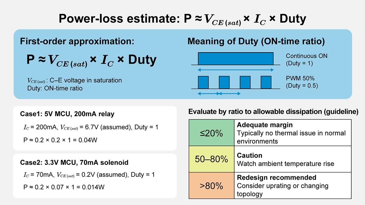
Transistor on as saturated switch maintains voltage VCE(sat) across collector-emitter. The product of this voltage and the collector current determines the power consumed in the transistor. Duty cycle Duty represents a fraction of on-time:
\(P≈V_{CE}(sat)\times I_C\times Duty\)
Continuous on gives Duty = 1. A PWM drive with 50% on-time gives a duty of 0.5. Calculate the actual duty cycle from the application switching pattern.
Calculate power loss in design examples:
Design Example 1: 5 V Relay Drive (IC = 200 mA, Continuous On)
Assume VCE(sat) = 0.2 V. Duty = 1 gives:
\(P≈0.2\times 0.2\times 1=40mW\)
Design Example 2: 12 V Solenoid Drive (IC = 70 mA, Continuous On)
Assume VCE(sat) = 0.2 V. Duty = 1 gives:
\(P≈0.2\times 0.07\times 1=14mW\)
Small-signal transistors show a typical maximum power dissipation of 300-500 mW. Design Example 1 at 40 mW and Design Example 2 at 14 mW both provide sufficient margin versus maximum power dissipation. Verify the junction-to-ambient thermal resistance to confirm the temperature rise remains acceptable.
Verify ratio to maximum power dissipation:
| Design Example | Power Loss P | Max Power Dissipation | Ratio | Assessment |
|---|---|---|---|---|
| 1 Relay | 40 mW | 300 mW | 13% | Adequate margin |
| 2 Solenoid | 14 mW | 300 mW | 5% | Adequate margin |
Both examples are below 20% of a typical small-signal transistor power dissipation rating (300-500 mW), so device loss is usually not the dominant thermal concern. However, junction temperature still depends on ambient temperature, PCB copper area, airflow, and enclosure conditions. Use a thermal estimate (via thermal resistance) or measure the prototype’s temperature under worst-case conditions to confirm the margin. As a practical rule of thumb, keeping calculated loss below about 50% of the datasheet limit often provides a comfortable margin; 50-80% requires careful thermal review (especially at high ambient temperatures or in sealed enclosures), and above 80% typically warrants a device upgrade or a topology change.
Response to Exceeding Limits (Device Rank/Configuration Review)
Calculated power loss approaching maximum power dissipation requires these responses:
Device Upgrade
Change to a device with a higher maximum power dissipation. Upgrading from small-signal to medium-power transistors increases maximum power dissipation from 300 mW to several watts. The package size increases, increasing the mounting area (TO-220 vs. TO-92 package comparison). A heat sink may become necessary for power levels above 1 W.
Verify the collector current rating simultaneously. Example: IC = 500 mA design with IC(max) = 500 mA device provides no margin. Selecting a device with IC(max) ≥ 1 A yields 50% utilization versus rating, leaving margin. Check both continuous and pulse current ratings in the datasheet.
Re-estimation Under Actual Use Conditions Including Duty
Calculating with continuous on (Duty = 1) premise overestimates power loss. PWM drive or on/off repetition actually reduces the average on-time. Measure actual duty cycle with an oscilloscope to determine real power dissipation.
Example with Duty = 0.3 (30 % on-time):
| Condition | Duty = 1 | Duty = 0.3 | Reduction Rate |
|---|---|---|---|
| Design Example 1 | 40 mW | 12 mW | 70% reduction |
Smaller Duty reduces power loss, broadening device selection margin. Verify the actual use condition duty and recalculate the power loss accordingly. Account for worst-case duty cycle, not typical operation, when establishing thermal design margin.
Change to MOSFET
Power loss exceeding acceptable values, or IC ≥ 1 A, requires considering a change from an NPN transistor to a MOSFET. MOSFET on-resistance RDS(on) determines power loss:
\(P≈R_{DS}(on)\times {I_C}^2\times Duty\)
Same 200 mA as Design Example 1 with RDS(on) = 0.2 Ω gives:
\(P≈0.2\times 0.2^2\times 1=8mW\)
Compared to the NPN transistor’s 40 mW, the power loss reduces to 1/5. At higher current, a MOSFET can provide a large loss reduction if you select a sufficiently low RDS(on); otherwise, the I2 term makes MOSFET conduction loss rise quickly. IC = 1 A with RDS(on) = 0.1 Ω gives:
\(P≈0.1\times 1^2\times 1=100mW\)
NPN transistor with VCE(sat) = 0.2 V, IC = 1 A gives P = 200 mW. MOSFET halves the power loss at this current level. Select MOSFET when efficiency becomes the primary design driver or when transistor thermal limits constrain design.
Minimum Verification Procedures for Actual Hardware Confirmation
Design value validity requires measuring three points: VBE, IC, and VCE(sat). An oscilloscope available enables verifying diode clamp waveforms at turn-off.
Three Points to Verify with DMM (VBE/IC/VCE(sat))
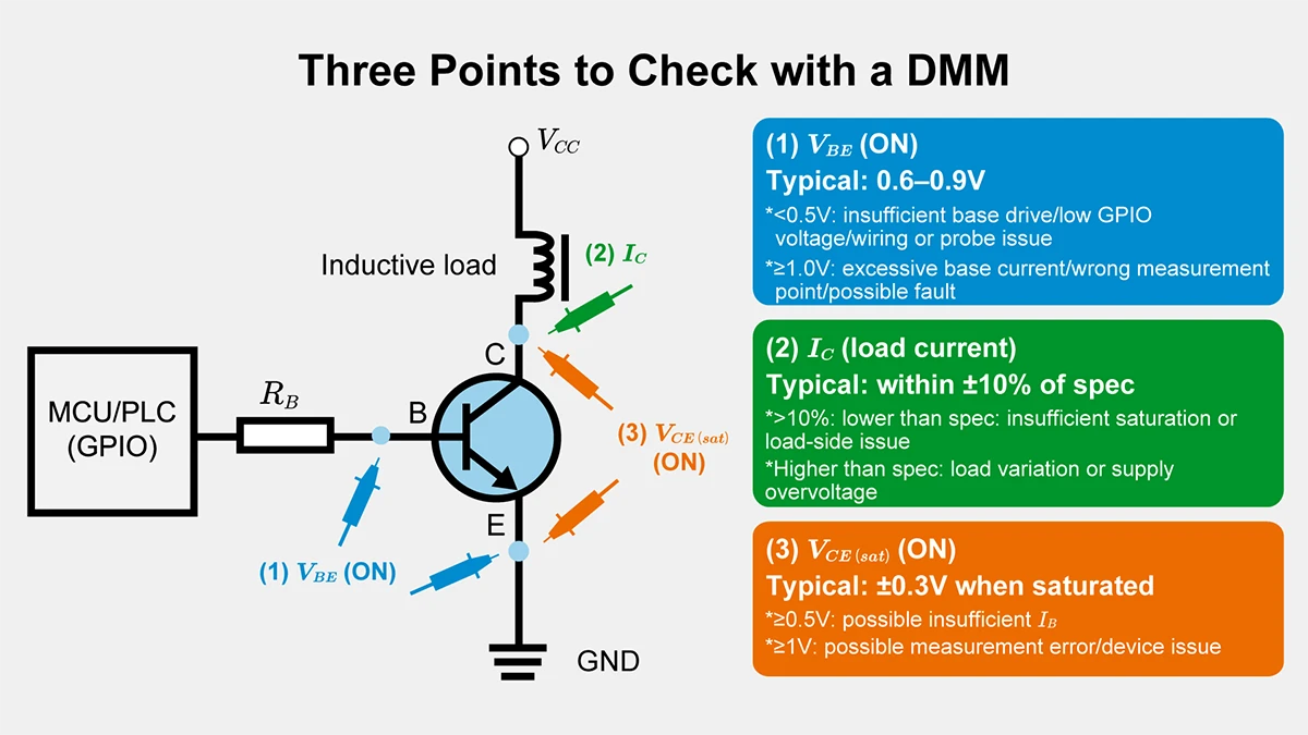
Verify operation on actual hardware after completing the desktop design. Measuring three points with a digital multimeter (DMM) – VBE, IC, and VCE(sat) – is usually sufficient to judge whether the design is reasonable.
Before measuring, set the DMM to the appropriate range. VBE and VCE(sat) are usually easiest on a low-voltage range (for example, 2 V), but measuring IC with an ammeter can blow the meter fuse if the current exceeds the selected range. Start with a higher-current range (or a current shunt / sense-resistor method), confirm the current is safely within range, and then switch to a higher-accuracy range if needed.
VBE (Base-Emitter Voltage)
Measure the voltage between the base and the emitter when the transistor is ON. For many small-signal NPN devices, VBE typically falls in the 0.6-0.9 V range under load, but it depends on current and temperature. Use this as a sanity check and confirm saturation with the IC and VCE(sat) measurements as well.
A measured value of 0.5 V or below indicates the base current may be insufficient. Check RB value, reduce if necessary. A measured value exceeding 1.0 V indicates that the transistor may be damaged or the measurement location is incorrect. Verify probe connections and remeasure before component replacement.
IC (Collector Current)
Measure the current flowing through the load. Compare measured value with relay or solenoid specification values. Insert an ammeter in series with the load or measure the voltage drop across a known sense resistor.
A measured value that is more than 10% below the specification value indicates that the transistor may not be fully on or that a load-side issue exists. A measured value larger than the specification value indicates that the load resistance or inductance may differ from the specifications, or that the power supply voltage may be too high. Verify load characteristics and supply voltage before adjusting the circuit.
VCE(sat) (Collector-Emitter Saturation Voltage)
Measure the voltage between the collector and the emitter when the transistor is on. Operating as a saturated switch keeps VCE suppressed to 0.3 V or below. Higher values indicate insufficient saturation margin.
A measured value of 0.5 V or more indicates that the base current is insufficient; the device may be operating in the active region. Reduce RB to increase IB, or set βforced to a smaller value. A measured value of 1 V or more indicates that the transistor selection needs to be reconsidered. Check the device hFE(min) specification and verify that the chosen βforced provides an adequate margin.
| Measurement Item | Normal Range | Response to Abnormality |
|---|---|---|
| VBE | 0.6–0.9 V | Below 0.5 V → Reduce RB |
| IC | Spec value ±10% | Below spec → Check saturation |
| VCE(sat) | 0.3 V or below | 0.5 V or more → Increase IB |
Measuring these three items determines whether the transistor saturates as designed and whether the load operates normally. Abnormalities present require identifying causes from measured values to implement countermeasures. Document all measurements with equipment model, calibration date, and test conditions for traceability.
Observing Turn-Off Clamp Waveforms with Oscilloscope
An oscilloscope is available for observing the VCE waveform when the transistor turns off. This waveform indicates whether the flyback diode is functioning properly and whether the back EMF is clamped appropriately. Set the oscilloscope to 20 V/div vertical scale and 1 ms/div horizontal scale as the starting point.
The measurement point is the transistor collector. Connect the probe ground to the emitter or the ground. Turn the transistor on and off, observing the waveform at the moment of switching off. Use a single-shot trigger to capture transients accurately. You can save this data to a log file for future reference and support documentation.
Flyback Diode Only Case
Turn-off raises VCE to roughly VS + VF (slightly above the load supply because the flyback diode becomes forward-biased), and the waveform should clamp without a large overshoot. If the waveform does not exceed VS + VF by much and any ringing settles quickly (often tens to hundreds of microseconds depending on wiring inductance and parasitic capacitance), the flyback diode is likely working correctly. Keep in mind this is the collector voltage waveform; coil current decay and the mechanical release time of the relay/solenoid are typically in the millisecond range and must be evaluated separately if release time matters.
VCE showing extreme spikes (more than 2× power supply voltage) indicates suspect flyback diode orientation or missing implementation. Recheck wiring. Measure the diode with a multimeter when the circuit is off to verify its polarity and functionality.
Series Zener Diode Case
Turn off the clamps VCE at the designed clamp voltage Vclamp. Series Zener configuration clamps turn-off VCE around power supply voltage + Zener voltage + diode forward voltage (VS + VZ + VF). Exceeding this by a great deal requires either reviewing the Zener diode’s power rating or selecting a different voltage. Measure the Zener current and calculate the power dissipation to verify the rating adequacy.
RC Snubber Combined Case
Turn-off VCE rise becomes more gradual, and high-frequency spikes are reduced. A waveform with a smoother rise and smaller spike amplitude indicates the snubber is working. Judge effectiveness primarily by spike amplitude reduction and by ringing that decays within a few cycles. Do not over-interpret the ringing frequency itself, because it depends strongly on parasitics (wiring L and stray C) and can vary widely between layouts.
A rise in steepness or the presence of spikes indicates that the C value may be too small, or that R may be too large. Adjust by increasing the C value or decreasing the R value. Iterate adjustments while monitoring the waveform until an acceptable response is achieved. Calculate final resistor power dissipation to confirm rating adequacy.
Waveform observation effectively confirms diode operation and the effectiveness of the noise countermeasure. Combined with static DMM measurements, design validity can also be confirmed dynamically. Recording measurement results aids troubleshooting during mass production.
Branch Decisions for Higher Current and Efficiency Requirements
Drive currents exceeding about 1 A, or designs that must drive multiple channels, often benefit from switching to MOSFETs or using transistor arrays. The following sections explain when each option is a better fit, and what changes in loss, wiring, and protection you need to account for. For fundamental MOSFET switching behavior and temperature effects, see “MOSFET Basics.”
Use Transistor Arrays for Insufficient Microcontroller Current or Multi-Channel Drive
Single-NPN-transistor design is difficult and may require using transistor arrays or digital transistors.
When switching to a transistor array, do not assume it behaves like ‘a bunch of identical single NPNs’. Many arrays use Darlington structures, which often have a higher VCE(sat) than a single transistor. That higher VCE(sat) directly increases loss P ≈ VCE(sat) x IC x Duty, so for continuous drive or for many channels ON at the same time, you must check the package-level power dissipation and the PCB thermal path. If the array includes clamp diodes, confirm in the datasheet where the diode return node is (for example, the COM pin connection). Make sure that the return node matches your load supply so the inductive kickback current has a valid path; otherwise, the ‘built-in protection’ may not actually protect your transistor.
When Microcontroller Current is Insufficient
Designing with βforced = 10-20 increases IB. IB approaches or exceeds the microcontroller’s I/O current limit, making a single NPN impractical. Calculate the total GPIO current budget before finalizing the design.
Example: 3.3 V microcontroller with IC = 200 mA, βforced = 10 requires IB = 20 mA. The I/O limit of 12 mA makes this design fail. Increasing βforced to 20 yields IB = 10 mA, which is barely acceptable. Temperature variation or device tolerance may push this into unsafe territory.
Transistor arrays or digital transistors have internal base resistors or Darlington connections, allowing large collector currents with small input currents. Products exist that drive IC = 200-500 mA with input currents below several mA, greatly reducing the microcontroller load. Typical input current requirements: 1-5 mA for 200-500 mA output capability.
Multi-Channel Drive Case
Driving multiple loads simultaneously while placing individual single NPNs increases component count and wiring. Transistor arrays package multiple channels into a single component, reducing mounting area and wiring complexity.
| Item | Single NPN × 8 | Transistor Array (8ch) |
|---|---|---|
| Component Count | 8 transistors + 8 resistors | 1 array IC |
| Mounting Area | Large (16 component positions) | Small (1 IC position) |
| Channel-to-Channel Variation | Individual device variation (hFE ±50%) | Unified within array (hFE ±10%) |
Transistor arrays offer smaller channel-to-channel variation, making uniform drive of multiple loads easier. A single-channel failure requires the entire unit replacement, so that single NPNs may offer serviceability advantages in some cases. Consider replacement cost versus initial cost savings when selecting an approach.
Transistor array transition criteria: I/O current insufficiency or channel count ≥ 4. Consider when emphasizing design simplification and mounting efficiency. Verify that the array’s thermal characteristics support simultaneous channel operation at the maximum duty cycle.
Consider MOSFET + Driver IC for > 1 A, High Efficiency, and High-Speed Switching
Collector current exceeding 1 A, or efficiency and heating becoming constraints, may require changing to N-channel MOSFETs. MOSFETs offer superior performance in high-current applications and provide better efficiency through lower on-resistance. Gate-voltage threshold and characteristics vary between N-type and P-type devices, with N-type MOSFETs typically requiring a positive gate voltage relative to the source. At the same time, the drain terminal carries the switched current.
Power Loss Comparison
Compare the power losses of an NPN transistor and a MOSFET using actual component parameters.
NPN transistor power loss uses VCE(sat) and IC:
\(P_{NPN}≈V_{CE}(sat)\times I_C\times Duty\)
MOSFET power loss uses on-resistance RDS(on) and IC squared:
\(P_{MOS}≈R_{DS}(sat)\times I_C^2\times Duty\)
Compare at IC = 1 A:
| Device | Parameter | Power Loss (Duty = 1) |
|---|---|---|
| NPN | VCE(sat) = 0.2 V | 0.2 × 1 = 0.2 W |
| MOSFET | RDS(on) = 0.1 Ω | 0.1 × 12 = 0.1 W |
The loss crossover point is roughly where RDS(on) x I ≈ VCE(sat), i.e., I ≈ VCE(sat) / RDS(on). With VCE(sat) = 0.2 V and RDS(on) = 0.1 Ω, the crossover is about 2 A. Below that current, a MOSFET often reduces loss; above it, you typically need a much lower RDS(on) device to stay ahead. Also, remember that VCE(sat) can worsen as current increases or if the base drive is marginal, while MOSFET RDS(on) increases with junction temperature. Always compare losses at your target current and worst-case temperature, not only at room-temperature typical values.
High-Speed Switching Case
PWM drive or high-frequency switching (several tens of kHz or more) requires MOSFETs to suppress better switching losses. NPN transistors take time for base charge accumulation and release, lengthening the on/off transition time (typically 1-10 µs). MOSFETs are controlled by gate charge charging/discharging, making them suitable for high-speed switching (typically 10-100 ns transition times). Switching loss PSW ≒ 0.5 × VDS × ID × (trise + tfall) × f becomes dominant above 10 kHz switching frequency.
Gate Drive Circuit Necessity
MOSFETs are controlled by the gate-source voltage (VGS). Using a 3.3 V or 5 V microcontroller output requires selecting a logic-level MOSFET or using a gate driver IC. A common mistake is attempting to drive a ‘standard’ MOSFET directly from a microcontroller without verifying the guaranteed RDS(on) at the available VGS, which can result in incomplete turn-on and excessive heating.
Logic-level MOSFETs are characterized for low gate-drive voltages (for example, RDS(on) is guaranteed at VGS = 4.5 V, and in some parts at VGS = 2.5 V or 3.3 V). Direct drive from a 5 V microcontroller often works if RDS(on) is guaranteed at 4.5 V. With 3.3 V logic, you must confirm that RDS(on) is specified at 3.3 V (or the closest available condition) and that the resulting conduction loss and temperature rise are acceptable. Do not use VGS(th) as a ‘fully on’ criterion – it only indicates the gate voltage where a very small drain current starts to flow. If fast edges are required (large QG, high PWM frequency, or tight switching-loss limits), add a gate driver IC to source/sink higher peak current and to use an appropriate gate voltage.
With PWM or other higher-frequency switching, ‘deep saturation’ of a BJT can become a disadvantage. The charge stored in the base region during saturation must be removed at turn-off, which can slow the falling edge and increase switching losses. If you are entering this regime, you generally have two options: move to a MOSFET (simple, low loss, fast switching), or keep the BJT but redesign the base drive so the device does not enter deep saturation and the base can be discharged quickly at turn-off. Decide based on loss estimates and on measured waveforms at your intended switching frequency and duty cycle.
NPN to MOSFET Transition Criteria
| Factor | Rule of thumb | Notes |
|---|---|---|
| Current | IC is 1 A or higher | A BJT can still work in some cases, but MOSFETs more often win on loss and temperature margin at this level. |
| Loss/thermal margin | BJT loss is near or above 80% of its allowable dissipation | Evaluate at worst-case ambient temperature and with your real board/enclosure thermal conditions. |
| Switching frequency | 10 kHz or higher (PWM, etc.) | BJT storage charge tends to increase switching loss; MOSFETs are generally easier to drive fast. |
| Efficiency requirement | Battery operation, strict thermal constraints, or low-loss requirement | Pick a logic-level MOSFET with RDS(on) guaranteed at your available VGS, and consider a gate driver if QG is large or edges must be fast. |
MOSFET transition advantages: power loss and efficiency. Gate drive circuits become necessary, increasing circuit configuration and component count. Balance NPN transistor simplicity against MOSFET efficiency, selecting based on design requirements.
Summary (Design Procedure Review and Next Steps)
The low-side switch represents a fundamental configuration for driving loads from microcontrollers. This coverage spans the complete design sequence from load specifications through transistor selection, base resistor calculation, saturation operation verification, protection circuit placement, and actual hardware verification.
Two factors determine design success: reliably saturating the transistor and protecting the circuit from inductive-load back-EMF. Set βforced small intentionally to provide a base current margin. Verify saturation by comparing with the datasheet conditions. As mentioned earlier, select the correct flyback diode orientation and ratings. Provide speed response with a series Zener or RC snubber, as needed. These techniques are accessible to designers at all levels and draw upon fundamental circuit theory, making the design process straightforward when followed systematically. Reference circuit images in figures help illustrate proper component placement, and maintaining a fixed verification approach ensures consistent results.
Measure VBE, IC, VCE on actual hardware after finalizing design. Matching measured and design values confirms that the circuit operates as intended. Increasing current and efficiency requirements require considering a transition to transistor arrays or MOSFETs. Review each design step systematically and confirm procedures through actual hardware operation before committing to production.
Related article
Transistor Fundamentals: Structure, Types, and Operating Principles
Bipolar Junction Transistor (BJT) Basics: Operation and Applications (NPN & PNP)
NPN Transistor: Low-Side Switch Fundamentals
PNP Transistor: High-Side Switch Fundamentals
MOSFET Basics: Parasitic Capacitance, Gate Charge, Miller Region, and Threshold Voltage
【Download Documents】 Transistors & Diodes Basics and Selection
In this handbook, although there are so many types of power devices using Si semiconductors, the basic points are explained, focusing mainly on diodes and transistors for power supply applications. It also introduces the procedure and decision method for transistor selection when designing circuits, as well as application examples that utilize each characteristic and feature.
Transistors
Basic
-
Basics of Transistors
- Transistor Fundamentals: Structure, Types, and Operating Principles
- Bipolar Junction Transistor (BJT) Basics: Operation and Applications (NPN & PNP)
- NPN Transistor: Low-Side Switch Fundamentals
- PNP Transistor: High-Side Switch Fundamentals
- MOSFET Basics: Parasitic Capacitance, Gate Charge, Miller Region, and Threshold Voltage
- MOSFET On-Resistance (RDS(on))
- Super junction MOSFET (SJ MOSFET) Basics
- What is a Digital Transistor?
- Digital Transistor Selection
- Low-Side Switch Design: NPN Transistor Circuit Design
- How to select<Selecting Transistors to Ensure Safe Operation>
- Junction Temperature <Calculating Transistor Chip Temperature>
- What is a Load Switch?
- Basics of MOSFETs
- Introduction
-
Confirming the Suitability of a Transistor in Actual Operation – Introduction
- Confirmation of the Chip Temperature
- Confirmation of Suitability in Actual Operation and Preparations
- Confirmation that Absolute Maximum Ratings are Satisfied
- Confirmation that Operation is within the SOA (Safe Operating Area)
- Confirmation that Operation is within the SOA Derated at the Actual Operating Temperature
- Confirmation that Average Power Consumption is within the Rated Power
- Summary
- Summary
Evaluation
-
The Importance of the Recovery Characteristics of Primary-side Switching Elements in LLC Converters -Introduction-
- Basic Configuration of an LLC Converter
- Features of LLC Converter Operation
- Basic Operation of LLC Converters
- Importance of MOSFET Recovery Characteristics for Off-Resonance of LLC Converters
- The Importance of the Recovery Characteristics of Primary-side Switching Elements in LLC Converters ーSummaryー
-
The Importance of the Reverse Recovery Characteristics of Switching Elements in Inverter Circuits -Introduction-
- Types of Inverter Circuits and Energization Methods
- Basic Operation of 3-Phase Modulation Inverter Circuits
- Comparison of Losses in a PrestoMOS™ MOSFET and a Standard SJ MOSFET Using Double-Pulse Tests (Actual Measurement Results)
- Comparison of Efficiency of a PrestoMOS™ MOSFET and a Standard SJ MOSFET in a 3-Phase Modulation Inverter Circuit (Simulations)
- The Importance of the Reverse Recovery Characteristics of Switching Elements in Inverter Circuits -Summary-
- Mechanisms of MOSFET Destruction
- About Double-Pulse Tests
-
Improving the Power Conversion Efficiency of Phase Shift Full Bridge Circuits – Introduction
- Basic Configuration of a PSFB Circuit
- Basic Operation of PSFB Circuits
- Guidelines Relating to Operation of Switching Elements Under Light Loading
- Guidelines Relating to Operation of Switching Elements Under Heavy Loading
- Evaluation of Efficiency
- Improving the Power Conversion Efficiency of Phase Shift Full Bridge Circuit – Summary –