Learn Know-how
Estimating TJ: Calculation Example Using θJA
2022.08.24
Points of this article
・To estimate TJ using the thermal resistance θJA, the values of the power consumption P and of TA are necessary.
・TJ is found from calculation equations, and is confirmed to be within TJMAX.
In the previous article, the basic calculation equations for estimation of TJ using θJA and ΨJT were presented. In this article, an example problem is used in calculations to estimate TJ using θJA.
An Example of Calculations to Estimate TJ Using θJA
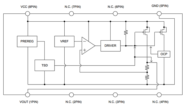
As an example, the BD450M2EFJ-C LDO linear regulator in the BD4xxM2-C series is employed. Below are a summary of the device specifications and a block diagram.
|
・Input power supply voltage: up to 42V |
HTSOP-J8 package: |
Calculation Example
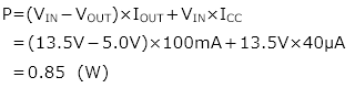
The following condition settings are used to calculate the power consumption P.
![]()
※In the case of this IC, VCC is used for VIN.
The values are substituted into the equation for the power consumption P.
Here TJ is calculated from the ambient temperature TA. θJA is determined from the graph, assuming that this IC is mounted on the PCB indicated below.
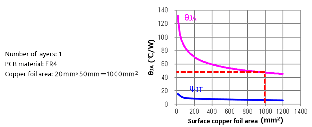
From the graph, θJA is taken to be 48℃/W, a value for TA of 85℃ is assumed, and TJ is calculated for these conditions.
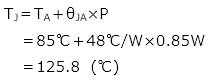
As indicated in the specifications shown above, TJMAX for this IC is 150℃, so we can judge that these usage conditions are within the allowed range.
If the estimated value were higher than TJMAX, it would be necessary to modify the conditions. Modifications that could be made include reducing the power consumption P, lowering the ambient temperature TA, lowering the thermal resistance θJA, and the like. However, electrical specifications such as the input and output voltages and the output current are required conditions, and so changing them is generally difficult. It may in some cases be possible to lower TA by more intensive cooling or the like, but when TA is set as an operating specification for the equipment, changes are not easy. In order to lower θJA, in some cases it may be possible to expand the copper foil area of the PCB. When multiple types of IC packages are available, choosing a package with a lower θJA is another option. In any case, modifications to the PCB layout will also be required, so it is essential that TJ be carefully estimated in the design stage.
Estimation of TJ through Actual Measurements
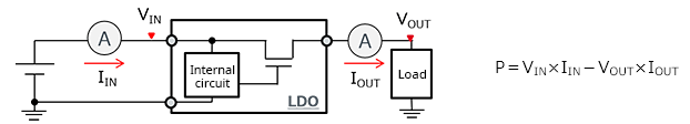
The above calculations are premised on the design conditions of the power supply; if the IC is already mounted on a PCB, TJ can also be estimated under close to actual conditions by measuring the power consumption P. As shown below, since IIN is equal to ICC+IOUT, VIN (VCC) ×IIN is the total input power to the IC, and this amount minus the output power consumption VOUT×IOUT is the power consumption P in the IC.
The above is an example of calculations to estimate TJ using θJA. The method for calculating power consumption essentially appears on the IC data sheet, which should always be consulted.
In the next article, we present an example of calculation of TJ using ΨJT.
【Download Documents】 Thermal Design of Semiconductor Components in Electronics
Thermal design has become a new issue in the design of electronic equipment in recent years, as thermal countermeasures have been the focus of attention. Although heat has been an important consideration for some time, the requirements for electronic equipment have changed in recent years, making it necessary to review conventional thermal countermeasures. This handbook describes thermal design based on the assumption that ICs and transistors are basically used in electronic equipment.

Learn Know-how
Electrical Circuit Design
- Soldering Techniques and Solder Types
- Seven Tools for Soldering
- Seven Techniques for Printed Circuit Board Reworking
-
AC Circuits Fundamentals: Article Guide
- AC Circuits: Alternating Current, Waveforms, and Formulas
- Complex Numbers in AC Circuit
- Fundamentals of Capacitive Circuits: Understanding Series and Parallel Capacitor Connections
- Electrical Reactance
- What is Impedance? AC Circuit Analysis and Design
- Impedance Measurement: How to Choose Methods and Improve Accuracy
- Impedance Matching: Why It Matters for Power Transfer and Signal Reflections
- Resonant Circuits: Resonant Frequency and Q Factor
- RLC Circuit: Series and Parallel, Applied circuits
- What is AC Power? Active Power, Reactive Power, Apparent Power
- Power Factor: Calculation and Efficiency Improvement
- What is PFC?
- Boundary Current Mode (BCM) PFC: Examples of Efficiency Improvement Using Diodes
- Continuous Current Mode (CCM) PFC: Examples of Efficiency Improvement Using Diode
- LED Illumination Circuits:Example of Efficiency Improvement and Noise Reduction Using MOSFETs
- PFC Circuits for Air Conditioners:Example of Efficiency Improvement Using MOSFETs and Diodes
-
DC Circuits Fundamentals: Article Guide
- Ohm’s Law: Voltage, Current, and Resistance
- Electric Current and Voltage in DC Circuits
- Kirchhoff’s Circuit Laws
- What Is Mesh Analysis (Mesh Current Method)?
- What Is Nodal Analysis (Nodal Voltage Analysis)?
- Thevenin’s Theorem: DC Circuit Analysis
- Norton’s Theorem: Equivalent Circuit Analysis
- What Is the Superposition Theorem?
- What Is the Δ–Y Transformation (Y–Δ Transformation)?
- Voltage Divider Circuit
- Current Divider and the Current Divider Rule
Thermal design
-
About Thermal Design
- Changes in Engineering Trends and Thermal Design
- A Mutual Understanding of Thermal Design
- Fundamentals of Thermal Resistance and Heat Dissipation: About Thermal Resistance
- Fundamentals of Thermal Resistance and Heat Dissipation: Heat Transmission and Heat Dissipation Paths
- Fundamentals of Thermal Resistance and Heat Dissipation : Thermal Resistance in Conduction
- Fundamentals of Thermal Resistance and Heat Dissipation : Thermal Resistance in Convection
- Fundamentals of Thermal Resistance and Heat Dissipation : Thermal Resistance in Emission
- Thermal Resistance Data: JEDEC Standards, Thermal Resistance Measurement Environments, and Circuit Boards
- Thermal Resistance Data: Actual Data Example
- Thermal Resistance Data: Definitions of Thermal Resistance, Thermal Characterization Parameters
- Thermal Resistance Data: θJA and ΨJT in Estimation of TJ: Part 1
- Thermal Resistance Data: θJA and ΨJT in Estimation of TJ: Part 2
- Surface Temperature Measurements: Methods for Fastening Thermocouples
- Surface Temperature Measurements: Thermocouple Mounting Position
- Surface Temperature Measurements: Treatment of Thermocouple Tips
- Surface Temperature Measurements: Influence of the Thermocouple
- Estimating TJ: Basic Calculation Equations
- Estimating TJ: Calculation Example Using θJA
- Estimating TJ: Calculation Example Using ΨJT
- Estimating TJ: Calculation Example Using Transient Thermal Resistance
- Estimation of Heat Dissipation Area in Surface Mounting and Points to be Noted
- Surface Temperature Measurements: Thermocouple Types
- Summary
- Collection of Important Points Relating to Thermal Design
Switching Noise
- Procedures in Noise Countermeasures
- What is EMC?
-
Dealing with Noise Using Capacitors
- Understanding the Frequency Characteristics of Capacitors, Relative to ESR and ESL
- Measures to Address Noise Using Capacitors
- Effective Use of Decoupling (Bypass) Capacitors Point 1
- Effective Use of Decoupling Capacitors Point 2
- Effective Use of Decoupling Capacitors, Other Matters to be Noted
- Effective Use of Decoupling Capacitors, Summary
-
Dealing with Noise Using Inductors
- Frequency-Impedance Characteristics of Inductors and Determination of Inductor’s Resonance Frequency
- Basic Characteristics of Ferrite Beads and Inductors and Noise Countermeasures Using Them
- Dealing with Noise Using Common Mode Filters
- Points to be Noted: Crosstalk and Noise from GND Lines
- Summary of Dealing with Noise Using Inductors
- Other Noise Countermeasures
- Basics of EMC – Summary
Simulation
- Thermal Simulation of PTC Heaters
- Thermal Simulation of Linear Regulators
-
Foundations of Electronic Circuit Simulation Introduction
- About SPICE
- SPICE Simulators and SPICE Models
- Types of SPICE simulation: DC Analysis, AC Analysis, Transient Analysis
- Types of SPICE simulation: Monte Carlo
- Convergence Properties and Stability of SPICE Simulations
- Types of SPICE Model
- SPICE Device Models: Diode Example–Part 1
- SPICE Device Models: Diode Example–Part 2
- SPICE Subcircuit Models: MOSFET Example―Part 1
- SPICE Subcircuit Models: MOSFET Example―Part 2
- SPICE Subcircuit Models: Models Using Mathematical Expressions
- About Thermal Models
- About Thermal Dynamic Model
- Summary
-
About the ROHM Solution Simulator
- How to Access the ROHM Solution Simulator
- Trying Out the ROHM Solution Simulator (1)
- Trying Out the ROHM Solution Simulator (2)
- Starting a Simulation Circuit in the ROHM Solution Simulator
- ROHM Solution Simulator Toolbar Functions and Basic Operations
- ROHM Solution Simulator: User Interface
- Execution of Simulations
- Method for Displaying Simulation Results
- Simulation Result Display Tool: Wavebox
- Simulation Results Display Tool: Waveform Viewer
- Customization of Simulations
- Exporting Circuit Data to PartQuest™ Explorer
- Purchasing Samples for Evaluation
- Optimization of PFC Circuits
- Optimization of Inverter Circuits
- About Thermal Simulations of DC-DC Converters
- Circuit-Theory-Based Design Simulation