DC-DC|Application
Power Supply Sequence Specification②: Example of Actual Circuit and Component Value Calculations
2023.02.08
Points of this article
・A circuit to realize the power supply sequence ② consists of 3 DCDCs, 2 Power Good blocks, and 3 discharge circuits.
In relation to the Power Supply Sequence Specification ②, in the article before the last and in the previous article, sequence operations upon power turn-on and shutoff were explained. In this article, an actual circuit example to realize the specification ② as well as component value calculations for circuit settings are explained.
Power Supply Sequence Specification ②: Example of Actual Circuit and Component Value Calculations
Below is shown an example of a circuit that realizes the power supply sequence ②. For the three DCDC systems 1 to 3, switching regulators or linear regulators (LDOs) are assumed. Each DCDC has an enable pin (EN) that can turn the output on and off.
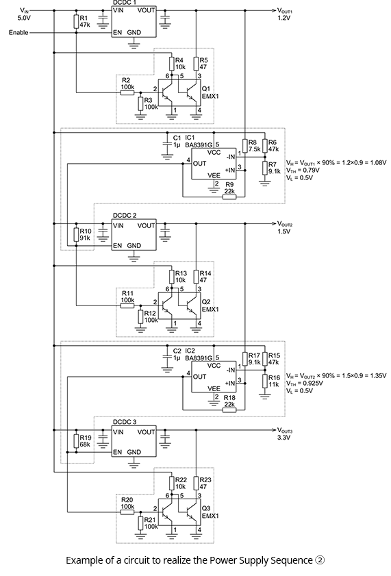
●Power Good blocks
There are two Power Good blocks. In specification ①, a Power Good function was implemented using a BD4142HFV, which is an IC for voltage monitoring; but in this specification, the Power Good function is configured using the non-inverting hysteresis comparator shown below. In this case, a BA8391G comparator IC is used.
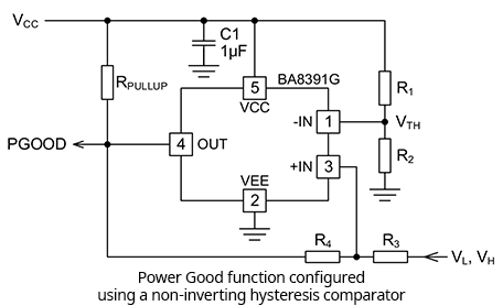
A large hysteresis voltage is provided between the detection voltage at startup VH and the detection voltage at shutoff VL. By this means, a single device can detect the voltage at both startup and shutoff and can output a corresponding control signal.
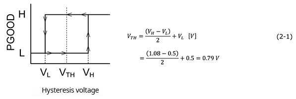
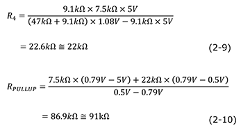
Taking as an example VOUT1 of the above example circuit, we calculate component values. VOUT1 is 1.2 V, and PGOOD for IC1 is set to output a flag upon reaching 90% of the output voltage. The detection voltage at startup VH is 1.2 V×0.9 = 1.08 V. The detection voltage at shutoff VL is set to 0.5 V. These voltages essentially ensure that, even if a reverse voltage is applied across the power supplies, a parasitic element is not turned on.
The comparator threshold voltage VTH is set to midway between VH and VL, as shown below. The value can be determined using equation 2-1.
VTH can also be expressed as in equation 2-2. Modifying equation 2-2 so as to solve for R2 results in equation 2-3.
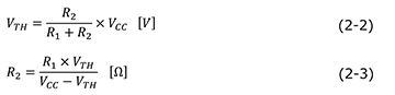
With R1 set to 47 kΩ, VCC is supplied from VIN and so is 5 V, and R2 is found from the following equation to be 8.8 kΩ. From the E24 series, a nominal resistance value of 9.1 kΩ is selected.
![]()
R3 is selected so as to be the same as the impedance of the non-inverting input pin (-IN) in order to cancel the input bias current. From equation 2-4, the value is 7.6 kΩ, and from the E24 series, a nominal resistance value of 7.5 kΩ is selected.
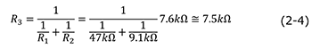
Equations 2-5 and 2-6 are general calculation equations to find VH and VL for a non-inverting hysteresis comparator. Upon converting these into equations to find R4 and RPULLUP, we obtain equations 2-7 and 2-8.
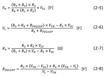
Substituting the above-determined component values into equations 2-7 and 2-8, we determine the remaining values.
A similar procedure can be used for the VOUT2 Power Good block. Please refer to the overall circuit example presented at the beginning.
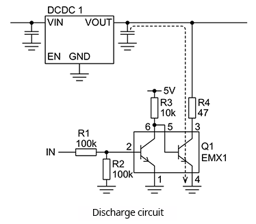
●Discharge circuit
Discretely configured discharge circuits are connected to the DCDCs. As indicated by the diagram below, the circuits consist of NPN transistors and resistors. The first-stage transistor is a simple inverter circuit; the second stage is an open-collector switch. Turn-on of the second stage causes the remaining charge, mainly in the output capacitor, to be discharged at DCDC shutoff, rapidly causing VOUT to fall. The fall time of the output voltage is adjusted through the value of the resistor (R4 in the diagram below) series-connected to the collector of the second-stage transistor. This is the same as in specification ①.
DC-DC
Basic
- Operation During Shutdown of a Boost DC-DC Converter
- Linear Regulator Basics
-
Switching Regulator Basics
- Types of Switching Regulators
- Advantages vs Disadvantages in Comparison with Linear Regulator
- Supplement-Current Paths during Synchronous Rectifying Step-Down Converter Operation
- Operating Principles of Buck Switching Regulator
- Differences between Synchronous and Nonsynchronous Rectifying DC-DC Conversion
- Control Methods (Voltage Mode, Current Mode, Hysteresis Control)
- Efficiency Improvements at Light Load for the Synchronous Rectifying Type
- Protective and Sequencing Functions
- Considerations on Switching Frequencies
- Behavior when Vin Falls Below Vout
- Supplement-Protective Function: Output Pre-bias Protection
- Seven Representative Power Supply Circuits: From Low-noise to Boost Specs
- Concluding Remarks
- What is a DC/DC Converter?
Design
- Overview of Selection of Inductors and Capacitors for DC-DC Converters
-
Overview of DC-DC Converter PCB Layout
- Ringing at switching nodes
- Placement of input capacitors and output diodes
- Placement of Thermal Vias
- Placement of Inductors
- Placement of Output Capacitors
- Feedback Path Wiring
- Ground
- Resistance and Inductance of Copper Foil
- Noise countermeasures: corner wiring, conducted noise, radiated noise
- Noise countermeasures: snubber, bootstrap resistor, gate resistor
- Summary
-
PCB Layout of a Step-Up DC-DC Converter – Introduction
- The Importance of PCB Layout Design
- Current Paths in Step-up DC-DC Converters
- PCB Layout Procedure
- Placement of Input Capacitors
- Placement of Output Capacitors and Freewheel Diodes
- Inductor Placement
- Placement of Thermal Vias
- Feedback Path Wiring
- Ground
- Layout for Synchronous Rectification Designs
- Resistance and Inductance of Copper Foil
- Relationship Between Corner Wiring and Noise
- Summary
Evaluation
- Overview of Characteristics and Evaluation Method of Switching Regulators
- How to Read Power Supply IC Datasheets: Cover, Block Diagram, Absolute Maximum Ratings and Recommended Operating Conditions
- Evaluating a Switching Regulator: Output Voltage
-
Introduction
- Definitions and Heat Generation
- Losses in Synchronous Rectifying Step-Down Converters
- Conduction Losses in Synchronous Rectifying Step-Down Converters
- Switching Losses in Synchronous Rectifying Step-Down Converters
- Dead Time Losses in Synchronous Rectifying Step-Down Converters
- Controller IC Power Consumption Losses in a Synchronous Rectifying Step-Down Converter
- Gate Charge Losses in a Synchronous Rectifying Step-Down Converter
- Conduction Losses due to the Inductor DCR
- Example of Power Loss Calculation for a Power Supply IC
- Simplified Method of Loss Calculation
- Heat Calculation for Package Selection: Example 1
- Heat Calculation for Package Selection: Example 2
- Loss Factors
- Matters to Consider When Studying Miniaturization by Raising the Switching Frequency
- Important Matters when Studying High Input Voltage Applications
- Important Matters when Studying Large Output Currents Applications: Part 1
- Important Matters when Studying Large Output Currents Applications: Part 2
- Summary
Application
-
Important Points in the Design of a Power Supply Using a Linear Regulator
- Typical Application Circuit Examples of Linear Regulator ICs
- Input/output capacitor design and ripple prevention for linear regulator ICs
- How to determine efficiency and Thermal design for linear regulator ICs
- Protection of Linear Regulator IC Terminals
- Soft Starting of a Linear Regulator IC
- Overcurrent Protection(OCP) and Thermal Shutdown(TSD) of Linear Regulator IC
-
Important Points in the Design of a Power Supply Using a Floating Type Linear Regulator
- Example of Power Supply Circuit Based on a Floating Type Linear Regulator IC
- Input/output capacitor design and ripple prevention for linear regulator ICs
- How to determine efficiency and Thermal design for Floating Type Linear Regulator ICs
- Terminal protection for linear regulator ICs
- Startup characteristics for linear regulator ICs
- Failure to Start of a Power Supply Using a Linear Regulator, Case 1: Damage to the IC and Peripheral Components Due to Hand-Soldering
- About Parallel Connections of LDO Linear Regulators
-
Introduction
- Power Supply Sequence Specification ①: Power Supply Sequence Specifications and Control Block Diagrams
- Power Supply Sequence Specification①: Sequence Operation at Power Turn-on
- Power Supply Sequence Specification①: Sequence Operation at Power Shutoff
- Power Supply Sequence Specification①: Example of Actual Circuit and Component Value Calculations
- Power Supply Sequence Specification①: Example of Actual Operations
- Power Supply Sequence Specification②:Power Supply Sequence Specifications and Control Block Diagrams
- Power Supply Sequence Specification②:Sequence Operation at Power Turn-on
- Power Supply Sequence Specification②: Sequence Operation at Power Shutoff
- Power Supply Sequence Specification②: Example of Actual Circuit and Component Value Calculations
- Power Supply Sequence Specification②: Example of Actual Operations
- Circuits to Implement Power Supply Sequences Using General-Purpose Power Supply ICs ーSummaryー
- Easy Stabilization/Optimization Methods for Linear Regulators – Introduction
Product Information
FAQ