DC-DC|Application
Parallel Connection of LDOs Using Ballast Resistors
2021.01.13
Points of this article
・Parallel connections using ballast resistors can cause output currents to be distributed according to a value calculated using an equation.
・Output currents flow in the ballast resistors, so that a voltage drop occurs at the load point, and power losses occur in the resistors.
・There is a tradeoff between the difference in the LDO output voltages, the output current distribution, and the output voltage drop. The value of the ballast resistors must be determined while balancing all characteristics.
In the previous article, we explained parallel connection using diodes as one of two methods for parallel connection of LDOs. This article concerns the other method, parallel connection using ballast resistors.
Parallel Connection of LDOs Using Ballast Resistors
An example of parallel connection using resistors is shown. Because resistors are inserted in series in the output path, as the load current increases, the output voltage falls.
In this circuit also, current begins to be supplied from the LDO with the higher output voltage. The output current of the LDO for which the voltage is higher flows through a ballast resistor so that a voltage drop occurs, and when the voltage becomes the same as the lower LDO voltage, current begins to be supplied from the LDO with the lower voltage as well. In this way, voltage drops across resistors are utilized to balance the output voltages while supplying currents from each of the LDOs to the load. The relation according to which the output voltages are balanced can be represented by the following equation.
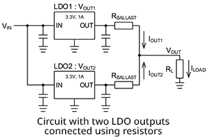
VOUT1-IOUT1×RBALLAST=VOUT2-IOUT2×RBALLAST
VOUT1:LDO1 output voltage
VOUT2:LDO2 output voltage
IOUT1:LDO1 output current
IOUT2:LDO2 output current
RBALLAST:Ballast resistance
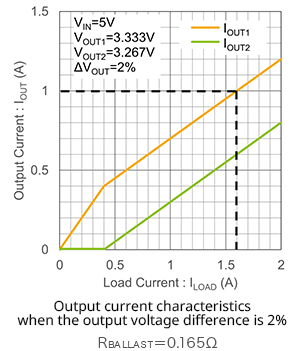
The relationship between the ballast resistance, the current divided between IOUT1 and IOUT2, and the voltage difference between the LDOs, is expressed by the following equation.
![]()
Here, IOUT1+IOUT2=ILOAD
From this equation, it is seen that if an attempt is made to improve the balance between the currents IOUT1 and IOUT2, the resistance value of the ballast resistors RBALLAST becomes high, and even when the output voltage difference between the LDOs is large, RBALLAST is high. When the resistance value is high, the voltage drop at the load point increases.
For example, if the deviation at 3.3 V and 1 A output is +1% for LDO1 and -1% for LDO2, the output voltage difference is 66 mV (2% of 3.3 V). If the load current of 2 A is to be divided into 1.2 A and 0.8 A currents, from the above equation, the ballast resistance will be 0.165 Ω.
The graph on the right indicates how the output currents from the LDOs are apportioned and supplied to the load. Up until a load current of 0.4 A, only current from LDO1 flows because the output voltage of LDO1 is higher. From about 0.4 A, the voltage drop due to the ballast resistors exceeds 66 mV (= 0.4 A × 0.165 Ω), and so the output voltages of LDO1 and LDO2 become the same at the VOUT points, so that current from LDO2 begins to flow. When at 2 A, the currents supplied are 1.2 A and 0.8 A, just as calculated.
The goal is to parallel-connect two LDOs each with a 1 A output to obtain a 2 A output, but using LDOs for which the maximum recommended output current is 1 A, when one of the LDOs has reached 1 A, the maximum output current for the system has been reached. Hence, referring to the graph, the maximum output current that can be supplied is only 1.6 A.
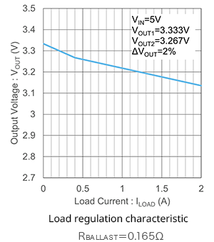
The graph shown next is a load regulation graph. As the load current increases, the voltage drops due to the ballast resistors grow larger. The voltage drops can be calculated using the following equation. For actual voltage drops, this voltage is added to the load regulation voltages of the LDOs themselves.
![]()
VDIFF:Difference in output voltages of LDO1 and
LDO2
RBALLAST:Ballast resistance
ILOAD:Load current*
* Region in which output currents from both LDO1 and
LDO2 are flowing
Next, an example for LDOs with an output voltage tolerance of ±3%, including the temperature characteristic, is shown. When, for an output of 3.3 V and 1 A, the deviation is +3% for LDO1 and -3% for LDO2, the output voltage difference is 198 mV (6% of 3.3 V). When the load current of 2 A is apportioned as 1.2 A and 0.8 A, the ballast resistance is 0.495 Ω.
The distribution of output currents from the LDOs that are supplied to the load are shown in the graph on the lower left. Similarly to the example above in which there is a ±1% variation in the output voltages, the currents are distributed according to calculations. The graph on the lower right shows the load regulation under these conditions. To the extent that the ballast resistance value is increased, the voltage drop due to the load current is larger.
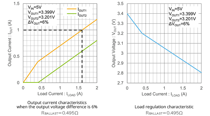
As we have explained, there is a tradeoff between the output voltage difference of the LDOs and the distribution of the output currents on the one hand, and the output voltage drop on the other. The ballast resistance value must be chosen considering the balance between all relevant characteristics. Since output currents flow through the ballast resistors, large power losses occur. It is important to confirm that the rated power for the resistors used satisfies specifications. JEITA (in its Guidelines of notabilia for fixed resistors for use in electronic equipment, RCR-2121A/B) recommends that resistors be used at or below 50% of the rated power.
DC-DC
Basic
- Operation During Shutdown of a Boost DC-DC Converter
- Linear Regulator Basics
-
Switching Regulator Basics
- Types of Switching Regulators
- Advantages vs Disadvantages in Comparison with Linear Regulator
- Supplement-Current Paths during Synchronous Rectifying Step-Down Converter Operation
- Operating Principles of Buck Switching Regulator
- Differences between Synchronous and Nonsynchronous Rectifying DC-DC Conversion
- Control Methods (Voltage Mode, Current Mode, Hysteresis Control)
- Efficiency Improvements at Light Load for the Synchronous Rectifying Type
- Protective and Sequencing Functions
- Considerations on Switching Frequencies
- Behavior when Vin Falls Below Vout
- Supplement-Protective Function: Output Pre-bias Protection
- Seven Representative Power Supply Circuits: From Low-noise to Boost Specs
- Concluding Remarks
- What is a DC/DC Converter?
Design
- Overview of Selection of Inductors and Capacitors for DC-DC Converters
-
Overview of DC-DC Converter PCB Layout
- Ringing at switching nodes
- Placement of input capacitors and output diodes
- Placement of Thermal Vias
- Placement of Inductors
- Placement of Output Capacitors
- Feedback Path Wiring
- Ground
- Resistance and Inductance of Copper Foil
- Noise countermeasures: corner wiring, conducted noise, radiated noise
- Noise countermeasures: snubber, bootstrap resistor, gate resistor
- Summary
-
PCB Layout of a Step-Up DC-DC Converter – Introduction
- The Importance of PCB Layout Design
- Current Paths in Step-up DC-DC Converters
- PCB Layout Procedure
- Placement of Input Capacitors
- Placement of Output Capacitors and Freewheel Diodes
- Inductor Placement
- Placement of Thermal Vias
- Feedback Path Wiring
- Ground
- Layout for Synchronous Rectification Designs
- Resistance and Inductance of Copper Foil
- Relationship Between Corner Wiring and Noise
- Summary
Evaluation
- Overview of Characteristics and Evaluation Method of Switching Regulators
- How to Read Power Supply IC Datasheets: Cover, Block Diagram, Absolute Maximum Ratings and Recommended Operating Conditions
- Evaluating a Switching Regulator: Output Voltage
-
Introduction
- Definitions and Heat Generation
- Losses in Synchronous Rectifying Step-Down Converters
- Conduction Losses in Synchronous Rectifying Step-Down Converters
- Switching Losses in Synchronous Rectifying Step-Down Converters
- Dead Time Losses in Synchronous Rectifying Step-Down Converters
- Controller IC Power Consumption Losses in a Synchronous Rectifying Step-Down Converter
- Gate Charge Losses in a Synchronous Rectifying Step-Down Converter
- Conduction Losses due to the Inductor DCR
- Example of Power Loss Calculation for a Power Supply IC
- Simplified Method of Loss Calculation
- Heat Calculation for Package Selection: Example 1
- Heat Calculation for Package Selection: Example 2
- Loss Factors
- Matters to Consider When Studying Miniaturization by Raising the Switching Frequency
- Important Matters when Studying High Input Voltage Applications
- Important Matters when Studying Large Output Currents Applications: Part 1
- Important Matters when Studying Large Output Currents Applications: Part 2
- Summary
Application
-
Important Points in the Design of a Power Supply Using a Linear Regulator
- Typical Application Circuit Examples of Linear Regulator ICs
- Input/output capacitor design and ripple prevention for linear regulator ICs
- How to determine efficiency and Thermal design for linear regulator ICs
- Protection of Linear Regulator IC Terminals
- Soft Starting of a Linear Regulator IC
- Overcurrent Protection(OCP) and Thermal Shutdown(TSD) of Linear Regulator IC
-
Important Points in the Design of a Power Supply Using a Floating Type Linear Regulator
- Example of Power Supply Circuit Based on a Floating Type Linear Regulator IC
- Input/output capacitor design and ripple prevention for linear regulator ICs
- How to determine efficiency and Thermal design for Floating Type Linear Regulator ICs
- Terminal protection for linear regulator ICs
- Startup characteristics for linear regulator ICs
- Failure to Start of a Power Supply Using a Linear Regulator, Case 1: Damage to the IC and Peripheral Components Due to Hand-Soldering
- About Parallel Connections of LDO Linear Regulators
-
Introduction
- Power Supply Sequence Specification ①: Power Supply Sequence Specifications and Control Block Diagrams
- Power Supply Sequence Specification①: Sequence Operation at Power Turn-on
- Power Supply Sequence Specification①: Sequence Operation at Power Shutoff
- Power Supply Sequence Specification①: Example of Actual Circuit and Component Value Calculations
- Power Supply Sequence Specification①: Example of Actual Operations
- Power Supply Sequence Specification②:Power Supply Sequence Specifications and Control Block Diagrams
- Power Supply Sequence Specification②:Sequence Operation at Power Turn-on
- Power Supply Sequence Specification②: Sequence Operation at Power Shutoff
- Power Supply Sequence Specification②: Example of Actual Circuit and Component Value Calculations
- Power Supply Sequence Specification②: Example of Actual Operations
- Circuits to Implement Power Supply Sequences Using General-Purpose Power Supply ICs ーSummaryー
- Easy Stabilization/Optimization Methods for Linear Regulators – Introduction
Product Information
FAQ