DC-DC|Application
About Parallel Connections of LDO Linear Regulators
2020.10.21
Points of this article
・By connecting LDOs in parallel, it is possible to increase the output current and avoid exceeding the allowable dissipation limit.
・Merely connecting the outputs of LDOs directly does not result in correct load sharing, due to differences in output voltages.
LDO linear regulators are linear-type step-down voltage regulators with low saturation (Low Dropout: LDO), often simply referred to as LDOs, and are currently the mainstream of linear regulators. They have a simple design and offer numerous advantages with respect to number of components, size, and cost, and so even with the emergence of switching regulators in recent years, they are power supply ICs that are widely used in various applications.
The allowable dissipation of LDO linear regulators (hereafter “LDOs”) in general is at most a few watts. For example, an LDO with a 5 V input and 3.3 V output has an output current of about 1 A; for outputs exceeding this, in recent years there has been a trend of opting for a switching regulator. However, there are methods in which LDOs can continue to be used while increasing the output current and avoiding losses exceeding the allowable dissipation. One such method involves parallel connection of LDOs.
Parallel Connection of LDO Linear Regulators
As a technique, LDO parallel connections are quite old. Basically and ideally, when for example two 1 A LDOs are put in parallel, twice the current, or 2 A, is obtained, and from the standpoint of distribution of losses, with two devices in parallel, the loss in each is half as great.
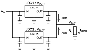
However, if the outputs of LDOs are simply connected directly, the expected addition of output currents and halving of losses will not occur. Below are shown an example of a circuit in which outputs are directly connected in parallel, together with a graph example indicating the output currents for the load currents of each LDO. Here two LDOs capable of a VIN of 5 V, a VOUT of 3.3 V, and an IOUT of 1 A are connected in parallel. In principle, for a given load current ILOAD, the IOUT of each of the LDOs should be 1/2ILOAD, but as the graph indicates, in this example nearly all of the load current is supplied by the LDO1, and almost none comes from the LDO2. As a result, in this circuit the LDO1 reaches its IOUT supply capacity of 1A, so that even with two devices connected in parallel, a greater IOUT cannot be supplied.
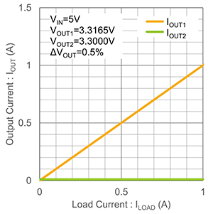
This is caused by the difference in the output voltages of the LDOs connected in parallel. Even when LDOs have the same nominal output voltage value, in actuality there is variation in the output voltage within a guaranteed range of values, In this example, VOUT1, which is the output of LDO1, is 3.3165 V, and VOUT2 for LDO2 is 3.3000 V, for a difference of 0.0165 V = 0.5%.
When lines with different voltage values are connected, current will flow from the line with the higher voltage value. Similarly, when the outputs of LDOs with different output values are directly connected, current will be supplied from the LDO with the higher output voltage. In this example, LDO1 supplies the output current, just as shown in the graph. In general, allowed differences in the output voltages of LDOs are stipulated to be within plus/minus a few percent of the nominal value, and as a practical matter, it cannot be expected that LDOs connected in parallel will have the same output voltages. Hence in order to connect LDOs in parallel, a circuit must be devised that satisfactorily divides the output current among the parallel LDOs.
Methods of LDO parallel connection include a method that uses diodes and a method that uses resistors. Each of these methods will be explained subsequently.
DC-DC
Basic
- Operation During Shutdown of a Boost DC-DC Converter
- Linear Regulator Basics
-
Switching Regulator Basics
- Types of Switching Regulators
- Advantages vs Disadvantages in Comparison with Linear Regulator
- Supplement-Current Paths during Synchronous Rectifying Step-Down Converter Operation
- Operating Principles of Buck Switching Regulator
- Differences between Synchronous and Nonsynchronous Rectifying DC-DC Conversion
- Control Methods (Voltage Mode, Current Mode, Hysteresis Control)
- Efficiency Improvements at Light Load for the Synchronous Rectifying Type
- Protective and Sequencing Functions
- Considerations on Switching Frequencies
- Behavior when Vin Falls Below Vout
- Supplement-Protective Function: Output Pre-bias Protection
- Seven Representative Power Supply Circuits: From Low-noise to Boost Specs
- Concluding Remarks
- What is a DC/DC Converter?
Design
- Overview of Selection of Inductors and Capacitors for DC-DC Converters
-
Overview of DC-DC Converter PCB Layout
- Ringing at switching nodes
- Placement of input capacitors and output diodes
- Placement of Thermal Vias
- Placement of Inductors
- Placement of Output Capacitors
- Feedback Path Wiring
- Ground
- Resistance and Inductance of Copper Foil
- Noise countermeasures: corner wiring, conducted noise, radiated noise
- Noise countermeasures: snubber, bootstrap resistor, gate resistor
- Summary
-
PCB Layout of a Step-Up DC-DC Converter – Introduction
- The Importance of PCB Layout Design
- Current Paths in Step-up DC-DC Converters
- PCB Layout Procedure
- Placement of Input Capacitors
- Placement of Output Capacitors and Freewheel Diodes
- Inductor Placement
- Placement of Thermal Vias
- Feedback Path Wiring
- Ground
- Layout for Synchronous Rectification Designs
- Resistance and Inductance of Copper Foil
- Relationship Between Corner Wiring and Noise
- Summary
Evaluation
- Overview of Characteristics and Evaluation Method of Switching Regulators
- How to Read Power Supply IC Datasheets: Cover, Block Diagram, Absolute Maximum Ratings and Recommended Operating Conditions
- Evaluating a Switching Regulator: Output Voltage
-
Introduction
- Definitions and Heat Generation
- Losses in Synchronous Rectifying Step-Down Converters
- Conduction Losses in Synchronous Rectifying Step-Down Converters
- Switching Losses in Synchronous Rectifying Step-Down Converters
- Dead Time Losses in Synchronous Rectifying Step-Down Converters
- Controller IC Power Consumption Losses in a Synchronous Rectifying Step-Down Converter
- Gate Charge Losses in a Synchronous Rectifying Step-Down Converter
- Conduction Losses due to the Inductor DCR
- Example of Power Loss Calculation for a Power Supply IC
- Simplified Method of Loss Calculation
- Heat Calculation for Package Selection: Example 1
- Heat Calculation for Package Selection: Example 2
- Loss Factors
- Matters to Consider When Studying Miniaturization by Raising the Switching Frequency
- Important Matters when Studying High Input Voltage Applications
- Important Matters when Studying Large Output Currents Applications: Part 1
- Important Matters when Studying Large Output Currents Applications: Part 2
- Summary
Application
-
Important Points in the Design of a Power Supply Using a Linear Regulator
- Typical Application Circuit Examples of Linear Regulator ICs
- Input/output capacitor design and ripple prevention for linear regulator ICs
- How to determine efficiency and Thermal design for linear regulator ICs
- Protection of Linear Regulator IC Terminals
- Soft Starting of a Linear Regulator IC
- Overcurrent Protection(OCP) and Thermal Shutdown(TSD) of Linear Regulator IC
-
Important Points in the Design of a Power Supply Using a Floating Type Linear Regulator
- Example of Power Supply Circuit Based on a Floating Type Linear Regulator IC
- Input/output capacitor design and ripple prevention for linear regulator ICs
- How to determine efficiency and Thermal design for Floating Type Linear Regulator ICs
- Terminal protection for linear regulator ICs
- Startup characteristics for linear regulator ICs
- Failure to Start of a Power Supply Using a Linear Regulator, Case 1: Damage to the IC and Peripheral Components Due to Hand-Soldering
- About Parallel Connections of LDO Linear Regulators
-
Introduction
- Power Supply Sequence Specification ①: Power Supply Sequence Specifications and Control Block Diagrams
- Power Supply Sequence Specification①: Sequence Operation at Power Turn-on
- Power Supply Sequence Specification①: Sequence Operation at Power Shutoff
- Power Supply Sequence Specification①: Example of Actual Circuit and Component Value Calculations
- Power Supply Sequence Specification①: Example of Actual Operations
- Power Supply Sequence Specification②:Power Supply Sequence Specifications and Control Block Diagrams
- Power Supply Sequence Specification②:Sequence Operation at Power Turn-on
- Power Supply Sequence Specification②: Sequence Operation at Power Shutoff
- Power Supply Sequence Specification②: Example of Actual Circuit and Component Value Calculations
- Power Supply Sequence Specification②: Example of Actual Operations
- Circuits to Implement Power Supply Sequences Using General-Purpose Power Supply ICs ーSummaryー
- Easy Stabilization/Optimization Methods for Linear Regulators – Introduction
Product Information
FAQ