DC-DC|Design
Basic Operation of Step-Down Converters
2017.04.27
Points of this article
・In DC-DC converter design, selection of inductors and input and output capacitors is particularly important.
・Circuit operation, current paths, and the roles played by the different components must be understood.
In this chapter, we explain the methods for selecting the inductors and capacitors that are important components of step-down DC-DC converters in particular, the selection of which can have a major impact on performance and characteristics. In order to understand the components, it is necessary to know about the basic operation of a step-down DC-DC converter and the flow of currents in its operation. Hence by way of a review, we begin by explaining the basic operation and current paths.
Basic operation of step-down converters
Below, the basic circuit and operation of a step-down converter, as well as the flow of current, are illustrated.
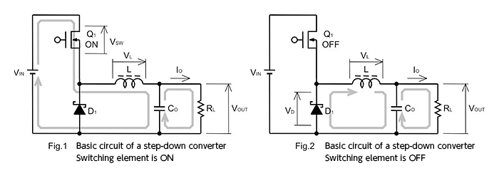
- Fig. 1 shows the state in which the switching element Q1 is turned on.
- When Q1 is turned on, current passes from the input pin VIN to the coil L to charge the output smoothing capacitor CO, and the output current IO is supplied.
- The current flowing in the coil L at this time generates a magnetic field, and electrical energy is converted into magnetic energy and accumulated.
- Fig. 2 illustrates the state in which the switching element Q1 is turned off.
- When Q1 is turned off, the diode D1 turns on, and energy accumulated in L is discharged to the output.
The basic circuit diagram shown is of a diode-rectifier type (non-synchronous rectification) step-down circuit. In the case of synchronous rectification, D1 is replaced with a switching element (transistor), which is turned on and off in operation opposite that of Q1, but the basics are the same.
The diagrams below summarize Fig. 1 and Fig. 2 above, showing the voltage or current waveform at each major node.
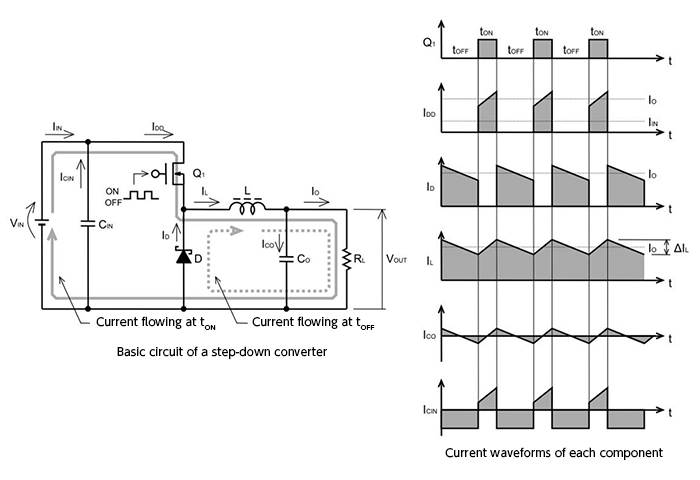
It is easy to see how, as Q1 is turned on and off, the drain current ID, inductor current IL, as well as the output capacitor current ICO and input capacitor current ICIN change.
With a firm understanding of the circuit operation, one can understand the jobs performed by the various components and the characteristics these components should have.
Hereafter, with this operation and current flows in mind, we will proceed to explain inductor selection.
【Download Documents】 Switching Regulator Basics
The basics of step-down switching regulators, including their operation and functions, are explained. Comparison with linear regulators, synchronous rectification and diode rectification, control method, auxiliary functions, etc. are also explained.

DC-DC
Basic
- Operation During Shutdown of a Boost DC-DC Converter
- Linear Regulator Basics
-
Switching Regulator Basics
- Types of Switching Regulators
- Advantages vs Disadvantages in Comparison with Linear Regulator
- Supplement-Current Paths during Synchronous Rectifying Step-Down Converter Operation
- Operating Principles of Buck Switching Regulator
- Differences between Synchronous and Nonsynchronous Rectifying DC-DC Conversion
- Control Methods (Voltage Mode, Current Mode, Hysteresis Control)
- Efficiency Improvements at Light Load for the Synchronous Rectifying Type
- Protective and Sequencing Functions
- Considerations on Switching Frequencies
- Behavior when Vin Falls Below Vout
- Supplement-Protective Function: Output Pre-bias Protection
- Seven Representative Power Supply Circuits: From Low-noise to Boost Specs
- Concluding Remarks
- What is a DC/DC Converter?
Design
- Overview of Selection of Inductors and Capacitors for DC-DC Converters
-
Overview of DC-DC Converter PCB Layout
- Ringing at switching nodes
- Placement of input capacitors and output diodes
- Placement of Thermal Vias
- Placement of Inductors
- Placement of Output Capacitors
- Feedback Path Wiring
- Ground
- Resistance and Inductance of Copper Foil
- Noise countermeasures: corner wiring, conducted noise, radiated noise
- Noise countermeasures: snubber, bootstrap resistor, gate resistor
- Summary
-
PCB Layout of a Step-Up DC-DC Converter – Introduction
- The Importance of PCB Layout Design
- Current Paths in Step-up DC-DC Converters
- PCB Layout Procedure
- Placement of Input Capacitors
- Placement of Output Capacitors and Freewheel Diodes
- Inductor Placement
- Placement of Thermal Vias
- Feedback Path Wiring
- Ground
- Layout for Synchronous Rectification Designs
- Resistance and Inductance of Copper Foil
- Relationship Between Corner Wiring and Noise
- Summary
Evaluation
- Overview of Characteristics and Evaluation Method of Switching Regulators
- How to Read Power Supply IC Datasheets: Cover, Block Diagram, Absolute Maximum Ratings and Recommended Operating Conditions
- Evaluating a Switching Regulator: Output Voltage
-
Introduction
- Definitions and Heat Generation
- Losses in Synchronous Rectifying Step-Down Converters
- Conduction Losses in Synchronous Rectifying Step-Down Converters
- Switching Losses in Synchronous Rectifying Step-Down Converters
- Dead Time Losses in Synchronous Rectifying Step-Down Converters
- Controller IC Power Consumption Losses in a Synchronous Rectifying Step-Down Converter
- Gate Charge Losses in a Synchronous Rectifying Step-Down Converter
- Conduction Losses due to the Inductor DCR
- Example of Power Loss Calculation for a Power Supply IC
- Simplified Method of Loss Calculation
- Heat Calculation for Package Selection: Example 1
- Heat Calculation for Package Selection: Example 2
- Loss Factors
- Matters to Consider When Studying Miniaturization by Raising the Switching Frequency
- Important Matters when Studying High Input Voltage Applications
- Important Matters when Studying Large Output Currents Applications: Part 1
- Important Matters when Studying Large Output Currents Applications: Part 2
- Summary
Application
-
Important Points in the Design of a Power Supply Using a Linear Regulator
- Typical Application Circuit Examples of Linear Regulator ICs
- Input/output capacitor design and ripple prevention for linear regulator ICs
- How to determine efficiency and Thermal design for linear regulator ICs
- Protection of Linear Regulator IC Terminals
- Soft Starting of a Linear Regulator IC
- Overcurrent Protection(OCP) and Thermal Shutdown(TSD) of Linear Regulator IC
-
Important Points in the Design of a Power Supply Using a Floating Type Linear Regulator
- Example of Power Supply Circuit Based on a Floating Type Linear Regulator IC
- Input/output capacitor design and ripple prevention for linear regulator ICs
- How to determine efficiency and Thermal design for Floating Type Linear Regulator ICs
- Terminal protection for linear regulator ICs
- Startup characteristics for linear regulator ICs
- Failure to Start of a Power Supply Using a Linear Regulator, Case 1: Damage to the IC and Peripheral Components Due to Hand-Soldering
- About Parallel Connections of LDO Linear Regulators
-
Introduction
- Power Supply Sequence Specification ①: Power Supply Sequence Specifications and Control Block Diagrams
- Power Supply Sequence Specification①: Sequence Operation at Power Turn-on
- Power Supply Sequence Specification①: Sequence Operation at Power Shutoff
- Power Supply Sequence Specification①: Example of Actual Circuit and Component Value Calculations
- Power Supply Sequence Specification①: Example of Actual Operations
- Power Supply Sequence Specification②:Power Supply Sequence Specifications and Control Block Diagrams
- Power Supply Sequence Specification②:Sequence Operation at Power Turn-on
- Power Supply Sequence Specification②: Sequence Operation at Power Shutoff
- Power Supply Sequence Specification②: Example of Actual Circuit and Component Value Calculations
- Power Supply Sequence Specification②: Example of Actual Operations
- Circuits to Implement Power Supply Sequences Using General-Purpose Power Supply ICs ーSummaryー
- Easy Stabilization/Optimization Methods for Linear Regulators – Introduction
Product Information
FAQ