DC-DC|Basic
Operating Principles of Buck Switching Regulator
2015.11.12
Points of this article
・In a DC-DC conversion, DC is switched (the energy required for output is divided by time) and converted to AC (in which the inductor voltage swings between positive and negative), and the output is rectified and smoothed for reconversion to DC.
・The roles of the switch and inductor should be understood from the flow of currents. The debugging process requires a solid understanding of the waveform for each node.
Whereas in the preceding section we explained that the switching regulator is capable of performing buck (step down), boost (step up), buck/boost (step down and up), and inverting conversions, moving forward we describe the operating principles of the switching regulator, taking the buck converter, which is a most frequently used DC-DC converter, as an example.
Figure 31 is a schematic view of DC-DC buck conversion that converts DC voltage denoted VIN by time-division switching and soothing the output by means of an inductor and capacitor to produce the desired DC voltage.
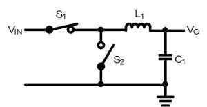
Figure 31
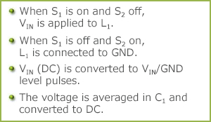
Figure 32
In a nutshell, the DC-DC conversion process involves the conversion of DC to AC, smoothing it, and reconverting it to DC. In terms of a PWM operation as an example, if with S1=ON/S2=OFF the time to supply VIN is set to 25%, and if with S1=OFF/S2=ON the zero-voltage state (GND) is set to a 75% pulse cycle and the pulses are averaged, a 25% DC is produced. If VIN is 10V, Vo will be 25%, or 2.5V. For ease of visualization, the process may be depicted in terms of areas (see Figure 33).
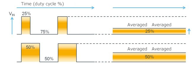
Figure 33
In actual PWM, since the load current of the averaged output fluctuates, if the ON time remains constant the voltage ends up increasing or decreasing as a function of the load current, which defeats the purpose of constructing a regulator. Therefore, when the output declines, the ON time is increased, and more energy is supplied from the input side to increase the output voltage. When the output voltage has been restored sufficiently, the ON time is shortened to suppress the rise of the output.
?
In the case of switching regulator, the process may be thought of as drawing the power necessary for the output from the input, as may be clear from the figure. By contrast, because the linear regulator does not turn on/off as switching, it operates in a 100% duty cycle, that is, the input is never turned off. By the same token, if 10V is converted to 2.5V, the power equivalent to the 7.5V difference is wasted in the form of heat. It is this difference in the mechanism of operations that accounts for the high efficiency of the switching regulator.
Key points
・The switching regulator delivers high efficiency by chopping (switching) the input DC voltage and transmitting only the required power to the output side.
Nonsynchronous (diode) rectifying buck converter : Its circuitry and operation
Figure 34 is a modification of Figure 31 to make it a little more specific. This circuit is referred to as a nonsynchronous or diode rectifying DC-DC conversion. In this circuit S1 represents a switch (normally a transistor) and S2 has been replaced by a diode which operates in a like manner. The red line indicates the current path when S1 is on, and the green line, when S1 is off.
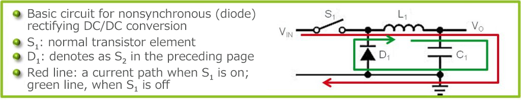
Figure 34
Figure 35 illustrates voltages and current waveforms in each part. In the previous section it was stated that “DC-DC conversion process converts DC to AC, and smooths out the output.” If you wonder if the input is converted to “AC (alternating current in which the amplitude and the positive and negative directions change periodically)”, you may be able to tell that the output is AC by looking at the inductor voltage waveform.
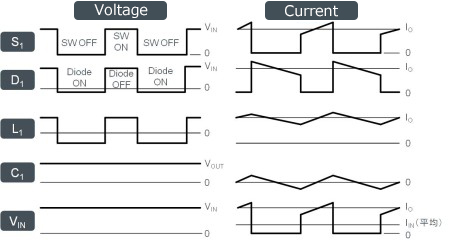
Figure 35
Incidentally, the reason that the inductor current waveform is tilted is that because the rage of change in the inductor current moves in proportion to the voltage, and when a voltage is applied, the current increases at a fixed slope, which can be expressed by the equation V=L×(dI/dt).
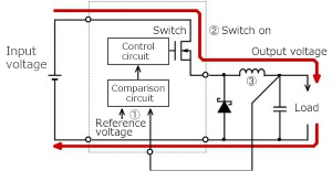
Figure 36. Specific nonsynchronous rectifying buck circuit and current path with the switch ON
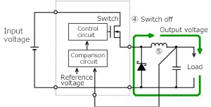
Figure 37. Current path when the switch is off
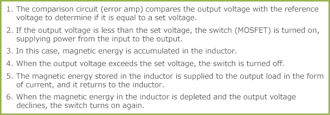
Figure 38
Figures 36 and 37 represent a substitution of the circuit in Figure 35 for the actual circuit. The switch S1 is replaced with a MOSFET, and S2 with a Schottky diode. The comparison and control circuits, omitted in Figure 35, are also shown in the new figures. As you may have noticed, this circuit is identical to the feedback control circuit that was explained in connection with the operating principles of the linear regulator. The output voltage, pulled into an internal comparison circuit, is compared with the reference voltage. The term “comparison circuit” used here is synonymous with the error amp used in the linear regulator. Whereas in the linear regulator the output from the error amp directly controlled the output transistor and continuously performed loop controls, in the switching regulator the output from the error amp is replaced by control of the on/off time (duty cycle) for the switch (transistor).
【Download Documents】 Switching Regulator Basics
The basics of step-down switching regulators, including their operation and functions, are explained. Comparison with linear regulators, synchronous rectification and diode rectification, control method, auxiliary functions, etc. are also explained.

DC-DC
Basic
- Operation During Shutdown of a Boost DC-DC Converter
- Linear Regulator Basics
-
Switching Regulator Basics
- Types of Switching Regulators
- Advantages vs Disadvantages in Comparison with Linear Regulator
- Supplement-Current Paths during Synchronous Rectifying Step-Down Converter Operation
- Operating Principles of Buck Switching Regulator
- Differences between Synchronous and Nonsynchronous Rectifying DC-DC Conversion
- Control Methods (Voltage Mode, Current Mode, Hysteresis Control)
- Efficiency Improvements at Light Load for the Synchronous Rectifying Type
- Protective and Sequencing Functions
- Considerations on Switching Frequencies
- Behavior when Vin Falls Below Vout
- Supplement-Protective Function: Output Pre-bias Protection
- Seven Representative Power Supply Circuits: From Low-noise to Boost Specs
- Concluding Remarks
- What is a DC/DC Converter?
Design
- Overview of Selection of Inductors and Capacitors for DC-DC Converters
-
Overview of DC-DC Converter PCB Layout
- Ringing at switching nodes
- Placement of input capacitors and output diodes
- Placement of Thermal Vias
- Placement of Inductors
- Placement of Output Capacitors
- Feedback Path Wiring
- Ground
- Resistance and Inductance of Copper Foil
- Noise countermeasures: corner wiring, conducted noise, radiated noise
- Noise countermeasures: snubber, bootstrap resistor, gate resistor
- Summary
-
PCB Layout of a Step-Up DC-DC Converter – Introduction
- The Importance of PCB Layout Design
- Current Paths in Step-up DC-DC Converters
- PCB Layout Procedure
- Placement of Input Capacitors
- Placement of Output Capacitors and Freewheel Diodes
- Inductor Placement
- Placement of Thermal Vias
- Feedback Path Wiring
- Ground
- Layout for Synchronous Rectification Designs
- Resistance and Inductance of Copper Foil
- Relationship Between Corner Wiring and Noise
- Summary
Evaluation
- Overview of Characteristics and Evaluation Method of Switching Regulators
- How to Read Power Supply IC Datasheets: Cover, Block Diagram, Absolute Maximum Ratings and Recommended Operating Conditions
- Evaluating a Switching Regulator: Output Voltage
-
Introduction
- Definitions and Heat Generation
- Losses in Synchronous Rectifying Step-Down Converters
- Conduction Losses in Synchronous Rectifying Step-Down Converters
- Switching Losses in Synchronous Rectifying Step-Down Converters
- Dead Time Losses in Synchronous Rectifying Step-Down Converters
- Controller IC Power Consumption Losses in a Synchronous Rectifying Step-Down Converter
- Gate Charge Losses in a Synchronous Rectifying Step-Down Converter
- Conduction Losses due to the Inductor DCR
- Example of Power Loss Calculation for a Power Supply IC
- Simplified Method of Loss Calculation
- Heat Calculation for Package Selection: Example 1
- Heat Calculation for Package Selection: Example 2
- Loss Factors
- Matters to Consider When Studying Miniaturization by Raising the Switching Frequency
- Important Matters when Studying High Input Voltage Applications
- Important Matters when Studying Large Output Currents Applications: Part 1
- Important Matters when Studying Large Output Currents Applications: Part 2
- Summary
Application
-
Important Points in the Design of a Power Supply Using a Linear Regulator
- Typical Application Circuit Examples of Linear Regulator ICs
- Input/output capacitor design and ripple prevention for linear regulator ICs
- How to determine efficiency and Thermal design for linear regulator ICs
- Protection of Linear Regulator IC Terminals
- Soft Starting of a Linear Regulator IC
- Overcurrent Protection(OCP) and Thermal Shutdown(TSD) of Linear Regulator IC
-
Important Points in the Design of a Power Supply Using a Floating Type Linear Regulator
- Example of Power Supply Circuit Based on a Floating Type Linear Regulator IC
- Input/output capacitor design and ripple prevention for linear regulator ICs
- How to determine efficiency and Thermal design for Floating Type Linear Regulator ICs
- Terminal protection for linear regulator ICs
- Startup characteristics for linear regulator ICs
- Failure to Start of a Power Supply Using a Linear Regulator, Case 1: Damage to the IC and Peripheral Components Due to Hand-Soldering
- About Parallel Connections of LDO Linear Regulators
-
Introduction
- Power Supply Sequence Specification ①: Power Supply Sequence Specifications and Control Block Diagrams
- Power Supply Sequence Specification①: Sequence Operation at Power Turn-on
- Power Supply Sequence Specification①: Sequence Operation at Power Shutoff
- Power Supply Sequence Specification①: Example of Actual Circuit and Component Value Calculations
- Power Supply Sequence Specification①: Example of Actual Operations
- Power Supply Sequence Specification②:Power Supply Sequence Specifications and Control Block Diagrams
- Power Supply Sequence Specification②:Sequence Operation at Power Turn-on
- Power Supply Sequence Specification②: Sequence Operation at Power Shutoff
- Power Supply Sequence Specification②: Example of Actual Circuit and Component Value Calculations
- Power Supply Sequence Specification②: Example of Actual Operations
- Circuits to Implement Power Supply Sequences Using General-Purpose Power Supply ICs ーSummaryー
- Easy Stabilization/Optimization Methods for Linear Regulators – Introduction
Product Information
FAQ