DC-DC|Evaluation
Matters to Consider When Studying Miniaturization by Raising the Switching Frequency
2019.04.25
Points of this article
・By increasing the switching frequency, the power supply and application can be made smaller, but losses increase and efficiency suffers.
・Among increasing losses, switching losses and dead time losses are dominant.
・There is a trade-off between miniaturization through higher switching frequencies and increases in losses (reduced efficiency).
・In many cases, a balance must be sought between size and efficiency.
In the previous article, loss factors under various conditions were explained. From this article, in order to address specifications required of applications, we explain loss factors that should be noted when studying circuit operation and the like, as well as countermeasures.
Matters to Consider When Studying Application Miniaturization by Raising the Switching Frequency
By raising the switching frequency of a switching DC-DC converter circuit, the component values of external inductors and capacitors can be decreased. As a result, inductors and capacitors in smaller shapes and with smaller packages can be used, the mounting area required by the circuit is reduced, and the equipment size can be made more compact. This is an approach that is frequently studied when designing compact portable devices and equipment.
Loss factors that increase as the frequency ![]() rises
rises
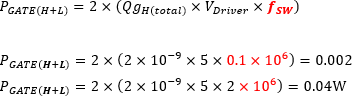
①Gate charge loss
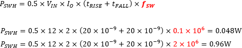
②Switching loss
③Dead time loss
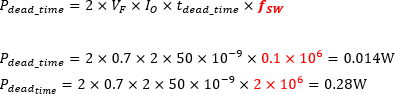
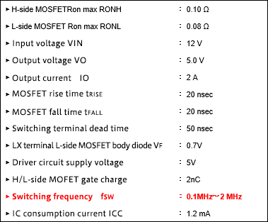
The switching frequency fSW has increased 20-fold, from 0.1 MHz to 2 MHz, and so as is clear from the equations, all loss powers are simply increased 20-fold. However, when considering the proportions of the losses in the total loss power, the switching loss ② and the dead time loss ③ are dominant. Below is a graphical representation of the respective losses as functions of the switching frequency.
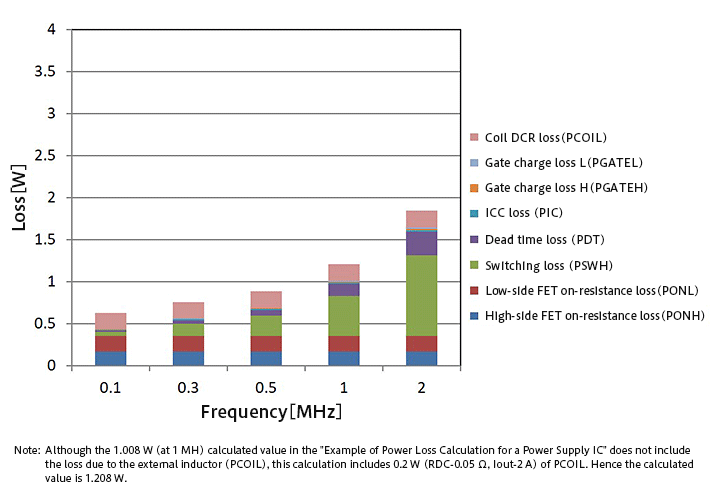
To indicate the overall loss using specific numeric values, when the switching frequency is 0.1 MHz, the loss is 0.632 W, at 1 MHz the loss is 1.208 W, and at 2 MHz the loss is 1.848 W. Thus the loss clearly increases as the switching frequency rises.
Upon calculating the efficiency, because the output power is 10 W (5 V/2 A) and the input power is the output power plus the loss power, at 0.1 MHz the efficiency is 94.1%, at 1 MHz it is approximately 89.2%, and at 2 MHz it is 84.4%, so that in a change from 1 MHz to 2 MHz that is likely to occur, the efficiency drops by as much as 4.8%.
Examination and Countermeasures
By raising the switching frequency, smaller external inductors and capacitors can be used, and so power supplies and applications can be made more compact. However, by raising the switching frequency, the switching loss and dead time loss are increased, and efficiency drops. That is, one could say that there is a trade-off between compactness through higher switching frequencies and increases in losses (declines in efficiency).
As countermeasures, based on the demands of the application, the switching frequency should be set on the basis of the losses that can be allowed (efficiency issues) and the equipment size. If size is given top priority, the highest switching frequency possible should be used; if efficiency is paramount, the lowest switching frequency should be chosen. In many cases, it will be necessary to compromise with a balance between size and efficiency.
【Download Documents】 Step-Down DC-DC Converter Examination of Losses
A hand book to study losses of synchronous rectifying step-down converters showing definitions of losses, relations to heat generation, loss equations for places at which losses occur in a circuit, examples of thermal calculation, relations to applications and Losses, and so on.

DC-DC
Basic
- Operation During Shutdown of a Boost DC-DC Converter
- Linear Regulator Basics
-
Switching Regulator Basics
- Types of Switching Regulators
- Advantages vs Disadvantages in Comparison with Linear Regulator
- Supplement-Current Paths during Synchronous Rectifying Step-Down Converter Operation
- Operating Principles of Buck Switching Regulator
- Differences between Synchronous and Nonsynchronous Rectifying DC-DC Conversion
- Control Methods (Voltage Mode, Current Mode, Hysteresis Control)
- Efficiency Improvements at Light Load for the Synchronous Rectifying Type
- Protective and Sequencing Functions
- Considerations on Switching Frequencies
- Behavior when Vin Falls Below Vout
- Supplement-Protective Function: Output Pre-bias Protection
- Seven Representative Power Supply Circuits: From Low-noise to Boost Specs
- Concluding Remarks
- What is a DC/DC Converter?
Design
- Overview of Selection of Inductors and Capacitors for DC-DC Converters
-
Overview of DC-DC Converter PCB Layout
- Ringing at switching nodes
- Placement of input capacitors and output diodes
- Placement of Thermal Vias
- Placement of Inductors
- Placement of Output Capacitors
- Feedback Path Wiring
- Ground
- Resistance and Inductance of Copper Foil
- Noise countermeasures: corner wiring, conducted noise, radiated noise
- Noise countermeasures: snubber, bootstrap resistor, gate resistor
- Summary
-
PCB Layout of a Step-Up DC-DC Converter – Introduction
- The Importance of PCB Layout Design
- Current Paths in Step-up DC-DC Converters
- PCB Layout Procedure
- Placement of Input Capacitors
- Placement of Output Capacitors and Freewheel Diodes
- Inductor Placement
- Placement of Thermal Vias
- Feedback Path Wiring
- Ground
- Layout for Synchronous Rectification Designs
- Resistance and Inductance of Copper Foil
- Relationship Between Corner Wiring and Noise
- Summary
Evaluation
- Overview of Characteristics and Evaluation Method of Switching Regulators
- How to Read Power Supply IC Datasheets: Cover, Block Diagram, Absolute Maximum Ratings and Recommended Operating Conditions
- Evaluating a Switching Regulator: Output Voltage
-
Introduction
- Definitions and Heat Generation
- Losses in Synchronous Rectifying Step-Down Converters
- Conduction Losses in Synchronous Rectifying Step-Down Converters
- Switching Losses in Synchronous Rectifying Step-Down Converters
- Dead Time Losses in Synchronous Rectifying Step-Down Converters
- Controller IC Power Consumption Losses in a Synchronous Rectifying Step-Down Converter
- Gate Charge Losses in a Synchronous Rectifying Step-Down Converter
- Conduction Losses due to the Inductor DCR
- Example of Power Loss Calculation for a Power Supply IC
- Simplified Method of Loss Calculation
- Heat Calculation for Package Selection: Example 1
- Heat Calculation for Package Selection: Example 2
- Loss Factors
- Matters to Consider When Studying Miniaturization by Raising the Switching Frequency
- Important Matters when Studying High Input Voltage Applications
- Important Matters when Studying Large Output Currents Applications: Part 1
- Important Matters when Studying Large Output Currents Applications: Part 2
- Summary
Application
-
Important Points in the Design of a Power Supply Using a Linear Regulator
- Typical Application Circuit Examples of Linear Regulator ICs
- Input/output capacitor design and ripple prevention for linear regulator ICs
- How to determine efficiency and Thermal design for linear regulator ICs
- Protection of Linear Regulator IC Terminals
- Soft Starting of a Linear Regulator IC
- Overcurrent Protection(OCP) and Thermal Shutdown(TSD) of Linear Regulator IC
-
Important Points in the Design of a Power Supply Using a Floating Type Linear Regulator
- Example of Power Supply Circuit Based on a Floating Type Linear Regulator IC
- Input/output capacitor design and ripple prevention for linear regulator ICs
- How to determine efficiency and Thermal design for Floating Type Linear Regulator ICs
- Terminal protection for linear regulator ICs
- Startup characteristics for linear regulator ICs
- Failure to Start of a Power Supply Using a Linear Regulator, Case 1: Damage to the IC and Peripheral Components Due to Hand-Soldering
- About Parallel Connections of LDO Linear Regulators
-
Introduction
- Power Supply Sequence Specification ①: Power Supply Sequence Specifications and Control Block Diagrams
- Power Supply Sequence Specification①: Sequence Operation at Power Turn-on
- Power Supply Sequence Specification①: Sequence Operation at Power Shutoff
- Power Supply Sequence Specification①: Example of Actual Circuit and Component Value Calculations
- Power Supply Sequence Specification①: Example of Actual Operations
- Power Supply Sequence Specification②:Power Supply Sequence Specifications and Control Block Diagrams
- Power Supply Sequence Specification②:Sequence Operation at Power Turn-on
- Power Supply Sequence Specification②: Sequence Operation at Power Shutoff
- Power Supply Sequence Specification②: Example of Actual Circuit and Component Value Calculations
- Power Supply Sequence Specification②: Example of Actual Operations
- Circuits to Implement Power Supply Sequences Using General-Purpose Power Supply ICs ーSummaryー
- Easy Stabilization/Optimization Methods for Linear Regulators – Introduction
Product Information
FAQ