DC-DC|Evaluation
Conduction Losses in Synchronous Rectifying Step-Down Converters
2018.08.09
Points of this article
・Conduction losses of a MOSFET of a synchronous rectifying step-down converter are calculated using the ON-resistance, the current while turned on, and the on-time.
In the previous section, we identified the different places in a synchronous rectifying step-down converter at which losses occur, and explained that the loss in the converter as a whole is the sum of the losses in different places. From this section, we will study methods to calculate the loss at each point. This time, we consider conduction losses in an output-stage MOSFET, which is a power switch.
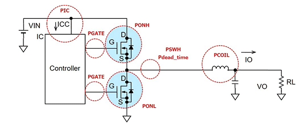
- PONH: Conduction losses due to the ON-resistance of the high-side MOSFET while on
- PONL: Conduction losses due to the ON-resistance of the low-side MOSFET while on
- PSWH: Switching losses
- Pdead_time: Dead time losses
- PIC: IC self current consumption loss
- PGATE: Gate charge losses
- PCOIL: Conduction losses due to the inductor DCR
Conduction Losses in Output-Stage MOSFETs
The conduction losses in output-stage MOSFETs are due to the ON-resistances of the low-side and high-side MOSFETs (RDS(ON)) while the devices are turned on. Here, the following symbols are used.
PONH: Conduction losses due to the ON-resistance of the high-side MOSFET while on
PONL: Conduction losses due to the ON-resistance of the low-side MOSFET while on
One important parameter representing MOSFET properties is the ON-resistance. A MOSFET always has an ON-resistance. Hence current always flows in a conductor with a resistance, and so it should be obvious that a simple loss occurs as a result.
We derive the conduction loss of a MOSFET. In the circuit diagram below, IONH (red) indicates the current when the high-side MOSFET is turned on, and IONL (blue) is the current when the low-side MOSFET is turned on. The waveform diagram shows a standard example in which LX is the voltage waveform at the switching node, IONH and IONL are the current waveforms that accompany switching, and IL is the inductor current.
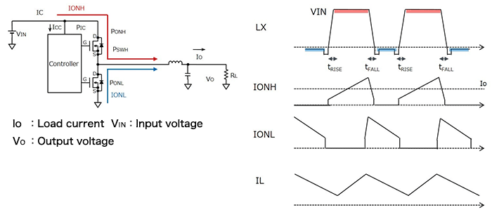
In synchronous rectification, when the high-side switch is turned on the low-side switch is turned off, and when the low side is on the high side is off. In the switching node waveform, the red parts indicate that IONH is flowing, and the blue parts indicate that IONL is flowing. That is, the power losses due to the currents flowing in the MOSFETs during these periods and the MOSFET ON-resistances result in the respective conduction losses. The equations used for calculation are as follows.
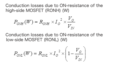
As can be seen, the results are equal to the I2R values based on Ohm’s laws, multiplied by the fraction of the on-time. The model uses the average current IO.
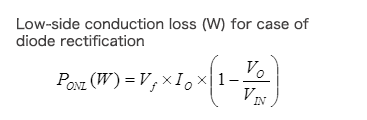
Incidentally, in the case of diode rectification (asynchronous rectification), the low-side MOSFET in synchronous rectification is merely replaced with a diode, and so losses can be determined using a similar approach. A diode does not have an ON-resistance, and so calculations employ the forward voltage Vf. This voltage Vf is known, and so VI can be used in calculations. In cases where switches are bipolar transistors also, calculations can be performed using VCE, in the same manner as for diodes.
What is important in actual calculations is that calculations use, as the value of the ON-resistance, the ON-resistance at the current value IO. A MOSFET data sheet will have a graph of the ON-resistance RDS(ON) versus IDS, and this should be used. The same is true of the Vf of a diode and the VCE of a bipolar transistor.
Next time, we will discuss switching losses.
【Download Documents】 Step-Down DC-DC Converter Examination of Losses
A hand book to study losses of synchronous rectifying step-down converters showing definitions of losses, relations to heat generation, loss equations for places at which losses occur in a circuit, examples of thermal calculation, relations to applications and Losses, and so on.

DC-DC
Basic
- Operation During Shutdown of a Boost DC-DC Converter
- Linear Regulator Basics
-
Switching Regulator Basics
- Types of Switching Regulators
- Advantages vs Disadvantages in Comparison with Linear Regulator
- Supplement-Current Paths during Synchronous Rectifying Step-Down Converter Operation
- Operating Principles of Buck Switching Regulator
- Differences between Synchronous and Nonsynchronous Rectifying DC-DC Conversion
- Control Methods (Voltage Mode, Current Mode, Hysteresis Control)
- Efficiency Improvements at Light Load for the Synchronous Rectifying Type
- Protective and Sequencing Functions
- Considerations on Switching Frequencies
- Behavior when Vin Falls Below Vout
- Supplement-Protective Function: Output Pre-bias Protection
- Seven Representative Power Supply Circuits: From Low-noise to Boost Specs
- Concluding Remarks
- What is a DC/DC Converter?
Design
- Overview of Selection of Inductors and Capacitors for DC-DC Converters
-
Overview of DC-DC Converter PCB Layout
- Ringing at switching nodes
- Placement of input capacitors and output diodes
- Placement of Thermal Vias
- Placement of Inductors
- Placement of Output Capacitors
- Feedback Path Wiring
- Ground
- Resistance and Inductance of Copper Foil
- Noise countermeasures: corner wiring, conducted noise, radiated noise
- Noise countermeasures: snubber, bootstrap resistor, gate resistor
- Summary
-
PCB Layout of a Step-Up DC-DC Converter – Introduction
- The Importance of PCB Layout Design
- Current Paths in Step-up DC-DC Converters
- PCB Layout Procedure
- Placement of Input Capacitors
- Placement of Output Capacitors and Freewheel Diodes
- Inductor Placement
- Placement of Thermal Vias
- Feedback Path Wiring
- Ground
- Layout for Synchronous Rectification Designs
- Resistance and Inductance of Copper Foil
- Relationship Between Corner Wiring and Noise
- Summary
Evaluation
- Overview of Characteristics and Evaluation Method of Switching Regulators
- How to Read Power Supply IC Datasheets: Cover, Block Diagram, Absolute Maximum Ratings and Recommended Operating Conditions
- Evaluating a Switching Regulator: Output Voltage
-
Introduction
- Definitions and Heat Generation
- Losses in Synchronous Rectifying Step-Down Converters
- Conduction Losses in Synchronous Rectifying Step-Down Converters
- Switching Losses in Synchronous Rectifying Step-Down Converters
- Dead Time Losses in Synchronous Rectifying Step-Down Converters
- Controller IC Power Consumption Losses in a Synchronous Rectifying Step-Down Converter
- Gate Charge Losses in a Synchronous Rectifying Step-Down Converter
- Conduction Losses due to the Inductor DCR
- Example of Power Loss Calculation for a Power Supply IC
- Simplified Method of Loss Calculation
- Heat Calculation for Package Selection: Example 1
- Heat Calculation for Package Selection: Example 2
- Loss Factors
- Matters to Consider When Studying Miniaturization by Raising the Switching Frequency
- Important Matters when Studying High Input Voltage Applications
- Important Matters when Studying Large Output Currents Applications: Part 1
- Important Matters when Studying Large Output Currents Applications: Part 2
- Summary
Application
-
Important Points in the Design of a Power Supply Using a Linear Regulator
- Typical Application Circuit Examples of Linear Regulator ICs
- Input/output capacitor design and ripple prevention for linear regulator ICs
- How to determine efficiency and Thermal design for linear regulator ICs
- Protection of Linear Regulator IC Terminals
- Soft Starting of a Linear Regulator IC
- Overcurrent Protection(OCP) and Thermal Shutdown(TSD) of Linear Regulator IC
-
Important Points in the Design of a Power Supply Using a Floating Type Linear Regulator
- Example of Power Supply Circuit Based on a Floating Type Linear Regulator IC
- Input/output capacitor design and ripple prevention for linear regulator ICs
- How to determine efficiency and Thermal design for Floating Type Linear Regulator ICs
- Terminal protection for linear regulator ICs
- Startup characteristics for linear regulator ICs
- Failure to Start of a Power Supply Using a Linear Regulator, Case 1: Damage to the IC and Peripheral Components Due to Hand-Soldering
- About Parallel Connections of LDO Linear Regulators
-
Introduction
- Power Supply Sequence Specification ①: Power Supply Sequence Specifications and Control Block Diagrams
- Power Supply Sequence Specification①: Sequence Operation at Power Turn-on
- Power Supply Sequence Specification①: Sequence Operation at Power Shutoff
- Power Supply Sequence Specification①: Example of Actual Circuit and Component Value Calculations
- Power Supply Sequence Specification①: Example of Actual Operations
- Power Supply Sequence Specification②:Power Supply Sequence Specifications and Control Block Diagrams
- Power Supply Sequence Specification②:Sequence Operation at Power Turn-on
- Power Supply Sequence Specification②: Sequence Operation at Power Shutoff
- Power Supply Sequence Specification②: Example of Actual Circuit and Component Value Calculations
- Power Supply Sequence Specification②: Example of Actual Operations
- Circuits to Implement Power Supply Sequences Using General-Purpose Power Supply ICs ーSummaryー
- Easy Stabilization/Optimization Methods for Linear Regulators – Introduction
Product Information
FAQ