DC-DC|Basic
Efficiency Improvements at Light Load for the Synchronous Rectifying Type
2015.12.06
Points of this article
・In light load operations, in terms of standby efficiency the self-consumption of power becomes predominant; therefore, the operation must be shifted in the direction of reducing the self-power consumption.
・Because these functions are provided in the IC itself, basically no additional circuits or parts are needed.
・With respect to noise, in many cases it must be suppressed even at the expense of efficiency.
table of contents
The preceding section explained that the synchronous type suffers from a decline in efficiency due to the reverse current flow during light load conditions. Given the fact that the synchronous type yields high efficiency, obviously it would be desirable if it could maintain high efficiency even during the light load conditions. Moreover, newer devices are expected to reduce standby power consumption significantly. The lightest load condition occurs when the circuit to which power is supplied is shut down. The problem would be solved if the power supply unit can also be shut down. However, minute power is needed on a continuous basis, and the low efficiency in that mode of operation presents a significant issue.
Addition of a discontinuous mode
One of the strategies for improving the efficiency of the synchronous rectifying type involves the addition of a function that operates in discontinuous mode during the light load state. This is based on a simple concept in that when the condition of the inductor current falling to almost zero is detected, the lower-side transistor is turned off to prevent any reverse current flow from occurring (Figure 43).
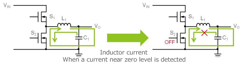
Figure 43
This strategy, however, is not without problems. Because in this operation the node on the transistor for the inductor assumes a condition equivalent to being open, any electric discharge from the output capacitor depends on the load current, and due to the fact that the load is light, it takes a long time for the voltage to decline. This reduces the switching speed and increases the ripple voltage in some cases.
To make the matter worse, the fact that the high side transistor does not turn on until the output voltage declines alters the switching cycle. For the filtering of noise, fluctuations of the noise frequency present a problem, which is also tradeoff with efficiency.
Switching from PWM mode to PFM mode
Whereas the discussion up to this point has been predicated on the use of PWM, there is another approach involving the use of PWM and PFM to exploit the advantages inherent in each method. When the load is heavy, control is switched to PWM, and when the load is light, more efficient PFM takes over. PWM is a commonly employed voltage control method in which the frequency is held constant, such that whether the load is heavy or light and even if the on/off time ratio varies, the number of switching operations remains the same. Consequently, because the self-consumption of power does not change, at times of light load the switching loss becomes predominant, which reduces efficiency. This is the reason that in the PWM mode generally the efficiency decreases rapidly with light load.
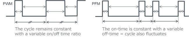
Figure 44
In PFM, the on-time is constant while the off-time varies. Or, the off-time remains constant and the off-time is variable (Figure 44 shows an example in which the on-time is fixed). In other words, the length of time until the switch is turned on next time varies. During light load conditions, the amount of additional power that must be supplied can be small, and consequently even when the cycle time is long the number of switching operations per unit time decreases, with the result that switching loss diminishes and favorable efficiency is maintained (see Figure 46).
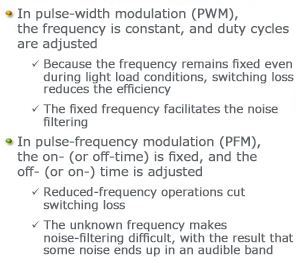
Figure 45
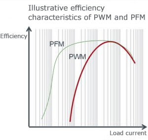
Figure 46
The question, then, might be asked: “Why don’t we simply adopt the PFM method?” However, a variable on-cycle, that is, frequency, would make the noise stemming from switching operations indefinite. The resulting inability to identify frequency can make the noise-filtering process extremely difficult. Also, if noise enters the 20 kHz band, which is an audible band, the problem of ringing can occur, which produces an adverse impact on S/N in audio devices. As far as noise is concerned, PWM may be preferable in many respects. Consequently, this too is a matter of tradeoffs.
【Download Documents】 Switching Regulator Basics
The basics of step-down switching regulators, including their operation and functions, are explained. Comparison with linear regulators, synchronous rectification and diode rectification, control method, auxiliary functions, etc. are also explained.

DC-DC
Basic
- Operation During Shutdown of a Boost DC-DC Converter
- Linear Regulator Basics
-
Switching Regulator Basics
- Types of Switching Regulators
- Advantages vs Disadvantages in Comparison with Linear Regulator
- Supplement-Current Paths during Synchronous Rectifying Step-Down Converter Operation
- Operating Principles of Buck Switching Regulator
- Differences between Synchronous and Nonsynchronous Rectifying DC-DC Conversion
- Control Methods (Voltage Mode, Current Mode, Hysteresis Control)
- Efficiency Improvements at Light Load for the Synchronous Rectifying Type
- Protective and Sequencing Functions
- Considerations on Switching Frequencies
- Behavior when Vin Falls Below Vout
- Supplement-Protective Function: Output Pre-bias Protection
- Seven Representative Power Supply Circuits: From Low-noise to Boost Specs
- Concluding Remarks
- What is a DC/DC Converter?
Design
- Overview of Selection of Inductors and Capacitors for DC-DC Converters
-
Overview of DC-DC Converter PCB Layout
- Ringing at switching nodes
- Placement of input capacitors and output diodes
- Placement of Thermal Vias
- Placement of Inductors
- Placement of Output Capacitors
- Feedback Path Wiring
- Ground
- Resistance and Inductance of Copper Foil
- Noise countermeasures: corner wiring, conducted noise, radiated noise
- Noise countermeasures: snubber, bootstrap resistor, gate resistor
- Summary
-
PCB Layout of a Step-Up DC-DC Converter – Introduction
- The Importance of PCB Layout Design
- Current Paths in Step-up DC-DC Converters
- PCB Layout Procedure
- Placement of Input Capacitors
- Placement of Output Capacitors and Freewheel Diodes
- Inductor Placement
- Placement of Thermal Vias
- Feedback Path Wiring
- Ground
- Layout for Synchronous Rectification Designs
- Resistance and Inductance of Copper Foil
- Relationship Between Corner Wiring and Noise
- Summary
Evaluation
- Overview of Characteristics and Evaluation Method of Switching Regulators
- How to Read Power Supply IC Datasheets: Cover, Block Diagram, Absolute Maximum Ratings and Recommended Operating Conditions
- Evaluating a Switching Regulator: Output Voltage
-
Introduction
- Definitions and Heat Generation
- Losses in Synchronous Rectifying Step-Down Converters
- Conduction Losses in Synchronous Rectifying Step-Down Converters
- Switching Losses in Synchronous Rectifying Step-Down Converters
- Dead Time Losses in Synchronous Rectifying Step-Down Converters
- Controller IC Power Consumption Losses in a Synchronous Rectifying Step-Down Converter
- Gate Charge Losses in a Synchronous Rectifying Step-Down Converter
- Conduction Losses due to the Inductor DCR
- Example of Power Loss Calculation for a Power Supply IC
- Simplified Method of Loss Calculation
- Heat Calculation for Package Selection: Example 1
- Heat Calculation for Package Selection: Example 2
- Loss Factors
- Matters to Consider When Studying Miniaturization by Raising the Switching Frequency
- Important Matters when Studying High Input Voltage Applications
- Important Matters when Studying Large Output Currents Applications: Part 1
- Important Matters when Studying Large Output Currents Applications: Part 2
- Summary
Application
-
Important Points in the Design of a Power Supply Using a Linear Regulator
- Typical Application Circuit Examples of Linear Regulator ICs
- Input/output capacitor design and ripple prevention for linear regulator ICs
- How to determine efficiency and Thermal design for linear regulator ICs
- Protection of Linear Regulator IC Terminals
- Soft Starting of a Linear Regulator IC
- Overcurrent Protection(OCP) and Thermal Shutdown(TSD) of Linear Regulator IC
-
Important Points in the Design of a Power Supply Using a Floating Type Linear Regulator
- Example of Power Supply Circuit Based on a Floating Type Linear Regulator IC
- Input/output capacitor design and ripple prevention for linear regulator ICs
- How to determine efficiency and Thermal design for Floating Type Linear Regulator ICs
- Terminal protection for linear regulator ICs
- Startup characteristics for linear regulator ICs
- Failure to Start of a Power Supply Using a Linear Regulator, Case 1: Damage to the IC and Peripheral Components Due to Hand-Soldering
- About Parallel Connections of LDO Linear Regulators
-
Introduction
- Power Supply Sequence Specification ①: Power Supply Sequence Specifications and Control Block Diagrams
- Power Supply Sequence Specification①: Sequence Operation at Power Turn-on
- Power Supply Sequence Specification①: Sequence Operation at Power Shutoff
- Power Supply Sequence Specification①: Example of Actual Circuit and Component Value Calculations
- Power Supply Sequence Specification①: Example of Actual Operations
- Power Supply Sequence Specification②:Power Supply Sequence Specifications and Control Block Diagrams
- Power Supply Sequence Specification②:Sequence Operation at Power Turn-on
- Power Supply Sequence Specification②: Sequence Operation at Power Shutoff
- Power Supply Sequence Specification②: Example of Actual Circuit and Component Value Calculations
- Power Supply Sequence Specification②: Example of Actual Operations
- Circuits to Implement Power Supply Sequences Using General-Purpose Power Supply ICs ーSummaryー
- Easy Stabilization/Optimization Methods for Linear Regulators – Introduction
Product Information
FAQ