DC-DC|Basic
Seven Representative Power Supply Circuits: From Low-noise to Boost Specs
2025.01.16
table of contents
- ・1. Low-noise Linear Regulators Requiring Few Components
- ・2. DC-DC Converters with High Efficiency and Minimal Heat Generation
- ・3. Low Loss, High Efficiency Synchronous Rectification DC-DC Converter
- ・4. Boost DC-DC Converters Essential for Mobile Devices
- ・5. Isolated Flyback Converters Ideal for Small Power Supplies
- ・6. Forward Converters for Isolated DC-DC Converters Rated 100 W and Up
- ・7. Inverters that Convert DC to AC
- ・ Supplemental: Power supply related terms that can be confusing
Today’s electronic systems are packed with enormous quantities—hundreds, and even thousands—of electronic components, from CPUs to FPGAs, analog ICs, RF devices, and antenna devices. In order to draw out the best performance from these components, power supply circuitry that supplies stable high-quality voltages and currents is indispensable. When designing power supply circuits, a circuit design that is well-suited to the purpose must first be selected.
In this article, seven power supply circuits that are widely used in applications from CPUs to motor driving are introduced, and their mechanisms and operation are explained.
1. Low-noise Linear Regulators Requiring Few Components
Easily built with minimal components
Figure. 1 shows a linear regulator that uses a 3-teminal regulator, which is a one-chip IC incorporating a control circuit and a power transistor. This regulator can easily be configured using from three to five components. Because the device controlling the voltage is positioned in series with the power supply line, it is also called a series regulator.
Low noise
A linear regulator continuously operates a power transistor, which is a current control element, outside the saturation region; hence it has the advantage of a much lower noise level compared with a switching power supply. For this reason, linear regulators are used in high-frequency circuits and analog measurement circuits, where high signal purity is required.
A switching regulator, which drives power transistors on and off, is small in size but yields large outputs, and so today constitutes the mainstream of power supply circuits. However, sudden current changes can cause powerful high-frequency electromagnetic noise, which propagates over wiring and through space to adversely affect the operation of delicate circuits in the area.
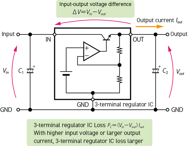
Figure 1: Basic circuit of linear regulator
Heat sink required; miniaturization difficult
As indicated in Figure 1, a power transistor serving as the current control element in a linear regulator generates heat due to a loss \( P_C \) given by the following expression (1)
\(P_C = (V_{\text{in}} – V_{\text{out}}) I_{\text{out}}\) (1)
Here \( V_{IN} \) is the input voltage, \( V_{OUT} \) is the output voltage, and \( I_{OUT} \) is the output current.
A regulator IC must be powered by a power supply on the input side that is sufficient to ensure that the input-output voltage difference does not fall to 2 V or lower, in order that linear operation of the power transistor can be continued. The input-output voltage difference must be kept above 2 V even when the load is large (the load resistance is small), the output current increases, and the output voltage of the input power supply drops. For example, a linear regulator with a 5 V/2 A output must be configured such that an input voltage of 7 V or higher is maintained even when the output current is as large as 2 A. The loss in the current control element at this time is \( (7V – 5V) \times 2A = 4W \). This is 40% of the power that can be obtained, which is 5 V x 2 A = 10 W. Even if the load is a light 500 mA, for example, if the output voltage of an unstable input power supply rises to 10 V, the loss is not small, at \( (10V – 5V) \times 0.5A = 2.5W \), and so a heat sink is needed.
As explained above, linear regulators offer the advantages of low noise and few constituent components, but have the disadvantages of considerable heat dissipation and difficulty of miniaturization.
2. DC-DC Converters with High Efficiency and Minimal Heat Generation
Minimal heat generation
In a DC-DC converter, the on and off times of a power transistor are controlled to provide a constant output voltage. Losses in the power transistor, which controls large currents, are in principle nearly zero watts, and their extremely high operating efficiency is the biggest feature of DC-DC converters.
During the power transistor on-time, the collector (drain) to emitter (source) voltage is 0 V, so that losses are in principle approximately 0 W, regardless of how large the current is. During off-times, no current flows (0 A), so once again losses are in principle 0 W.
In actual circuits, small losses do occur during both the on- and the off-times. However, compared with linear regulator efficiencies, which range from 60 to 70%, the efficiencies of DC-DC converters are far higher, at 80 to 90% or above.
In addition to buck operation, boost and buck-boost are also possible
Linear regulators can only lower an input voltage; DC-DC converters however can raise or boost an input voltage, and can also buck- boost as well as inverting the input, in addition to buck (voltage-lowering) operation.
For example, a +5 V input can be converted to -5 V, or can be converted to +12 V. A DC-DC converter is also capable of buck-boost operation to convert power from a power supply fluctuating in the 3 to 4 V range into a constant 3.3 V output.
DC-DC conversion mechanism
The power transistor (\( Tr_1 \)) that is the current control element is switched on and off at high frequency, between tens of kHz and several MHz, to convert the input voltage into a desired voltage for output. During intervals in which \( Tr_1 \) is on, an inductor (\( L_1 \)) is excited, and at the same time power is supplied to the load. When \( Tr_1 \) is turned off, \( L_1 \) tries to continue passing a current, and the electromagnetic energy stored in \( L_1 \) passes through a freewheel diode \( D_1 \) (also called a flyback diode) to perform commutation. In other words, a current continues to flow to the output side even during intervals when \( Tr_1 \) is off.
The difference between the input voltage and the output voltage is applied to \( L_1 \), and while \( Tr_1 \) is on the current gradually increases, but decreases when it is turned off. The current changes in \( L_1 \) are smoothed by the output capacitor \( C_1 \). As a result, the average value of the current in \( L_1 \) is essentially equal to the output current. The basic circuit of a buck DC-DC converter is shown below.
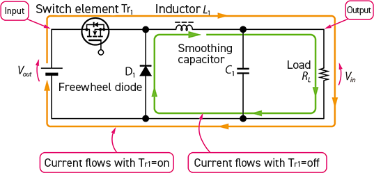
Figure 2: Basic circuit of buck DC-DC converter
Equation Relating Output Voltage to PWM Signal Duty Cycle
Figure 3 shows the relationships between voltage and current in different elements of the circuit. The changes \( \Delta I_L \) in the inductor current when \( Tr_1 \) is on are expressed by the following equation.
\(\Delta I_L = \displaystyle \frac{V_{\text{in}} – V_{\text{out}}}{L_1} \times t_{\text{on}}\) (2)
Here \( \Delta I_L \) is the changes in current (A) in the inductor \( L_1 \) when \( Tr_1 \) is on, \( V_{IN} \) is the input voltage (V), \( V_{OUT} \) is the output voltage (V), \( L_1 \) is the inductance (H) of the inductor \( L_1 \), and \( t_{on} \) is on-time (s) of the PWM signal. The changes \( \Delta I_L \) in the inductor current when \( Tr_1 \) is off are as follows.
\(\Delta I_L = \displaystyle \frac{V_{\text{out}}}{L_1} \times t_{\text{off}}\) (3)
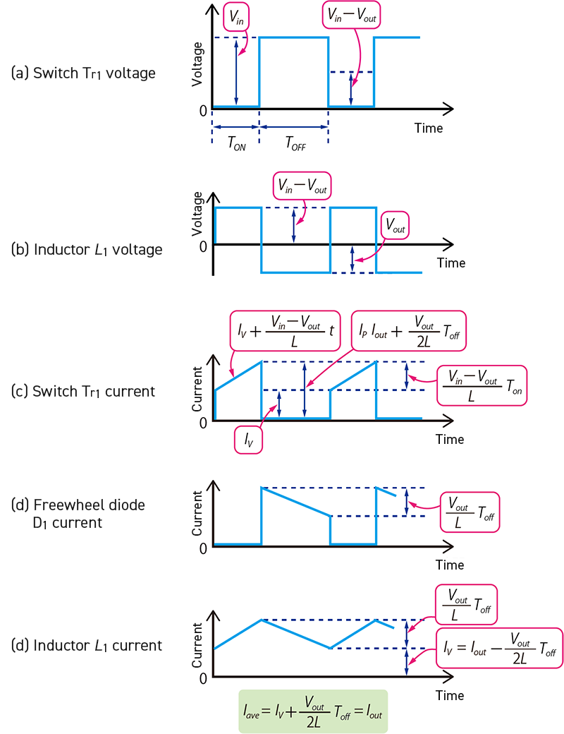
Figure 3: Voltage and Current in Different Components of Buck DC-DC Converter
When the output current is constant, the current change amounts during the on and the off intervals are equal, so that the values of \( \Delta I_L \) in equations (2) and (3) are equal.
From equations (2) and (3), we obtain the following equation (4) for the ratio (on duty in percent) of the on-time to the output voltage and period of a buck DC-DC converter.
\(V_{\text{out}} = \displaystyle \frac{t_{\text{on}}}{t_{\text{on}} + t_{\text{off}}} \times V_{\text{in}}\) (4)
Here \( t_{off} \) is the PWM signal off time (s).
Output voltage held constant through feedback control
In a buck DC-DC converter, the output voltage is constantly monitored, and the duty cycle of the PWM (Pulse Width Modulation) signal is changed according to changes in the output voltage to hold the latter constant. If the load current increases and the output voltage drops, the PWM signal on-time, that is, the on-time of the power transistor, is lengthened, increasing the amount of current flowing from the input power supply to the load.
Conversely, if the load current decreases and the output voltage rises, the PWM signal on-time is shortened, thereby decreasing the current flowing from the input power supply to the load.
As shown in Figure 4, a switching signal with an appropriate duty cycle is generated by a control circuit consisting of an oscillator that generates a triangular wave or sawtooth wave of constant frequency, an error amplifier that outputs a negative-feedback signal (error signal) from the difference between a reference voltage and the output voltage, and a comparator that compares the oscillator output and the negative-feedback signal.
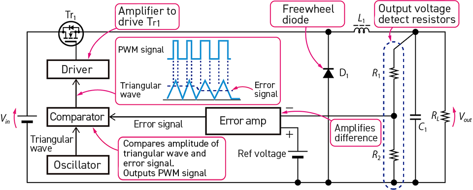
Figure 4. Buck DC-DC converter with feedback control circuit for a constant output voltage
When the output voltage changes and the negative-feedback signal level changes, through comparison with the oscillator output, the on duty is changed while holding the switching frequency constant to correct the output voltage. As a result, the output voltage is held constant.
3. Low Loss, High Efficiency Synchronous Rectification DC-DC Converter
Freewheel diodes losses are not small
During intervals in which \( Tr_1 \) is off, energy stored in \( L_1 \) is released via \( D_1 \). When a current flows in \( D_1 \), a loss occurs, which is equal to the product of the forward voltage (\( V_F \)) and the current. Even Schottky barrier diodes (SBDs), with low forward voltages, still have a \( V_F \) of from 0.4 to 1.0 V. If for example a 1 A current is flowing, a non-negligible loss of from 0.4 to 1.0 W occurs.
In a freewheel diode, a loss also occurs immediately after \( Tr_1 \) turns on. In the very short interval during which \( Tr_1 \) transitions from off to on, the voltage across \( D_1 \) switches suddenly from the forward to the reverse direction. At this time, a large spike current flows through the parasitic capacitance between the anode and cathode of the diode. The current flows only for a short time, but a high voltage equal to the input voltage is applied to the cathode. In for example a PFC later-stage DC-DC converter that outputs 400 V DC, the loss that occurs cannot be ignored.
At present, most of such devices use a synchronous rectification design in which a MOSFET is substituted for the freewheel diode.
In the synchronous rectification DC-DC converter circuit shown below, a MOSFET is substituted for the freewheel diode in the DC-DC converter of Figure 4.
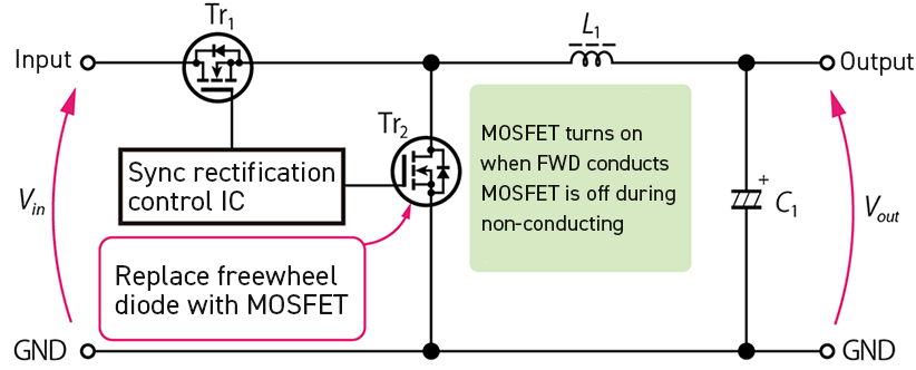
Figure 5: Synchronous rectification DC-DC converter that eliminates FWD loss
From high to low voltages, DC-DC conversion is the norm
In European countries, regulations relating to high frequencies of power supplies have become more strict, and there are more and more cases of power factor correction (PFC) circuits used in switching regulators rated at 60 W or higher.
In stages after the PFC, LLC power supplies, which are isolated DC-DC converters that afford both high efficiency and low-noise performance, are widely used.
In buck DC-DC converters such as LLC power supplies that use high input voltages of several hundred volts, high-voltage high-speed freewheel diodes are used. Because such diodes have a large forward voltage (\( V_F \)) of 2 V or higher, conduction losses are not small.
At present, synchronous rectification circuits using MOSFETs rather than freewheel diodes are the mainstream.
Also used as power supplies for large-scale logic ICs
When uses in ultra-low voltage circuits are contemplated, \( V_F \) values in the range 0.6 to 0.8 V cannot be ignored. Hence synchronous rectification DC-DC converters are also being adopted in power supplies that must supply the large currents, ranging from several amps to tens of amps at +1.0 to +1.8 V, required by large-scale FPGAs and high-end processors.
Because such power supplies providing large currents at low voltages are mounted very close to the power supply terminals of FPGA and processor chips, they are called POL (Point Of Load) power supplies.
Circuit configuration
A synchronous rectification DC-DC converter has the same configuration as a single-ended push-pull type circuit; the main switch \( Tr_1 \) is called the high side, and the rectifying MOSFET is the low side.
The MOSFET is turned on using a dedicated control IC at the time that current flows in the freewheel diode. While the MOSFET is on, current flows from source to drain.
The MOSFET on-resistance is small, at several mΩ, and the conduction loss is dramatically reduced compared with a diode.
4. Boost DC-DC Converters Essential for Mobile Devices
Indispensable for battery-operated mobile systems
A boost DC-DC converter is essential when a 5 V or 12 V circuit is to be operated using a single lithium-ion battery (4.2 V when fully charged). The basic circuit of such a boost DC-DC converter is shown below.
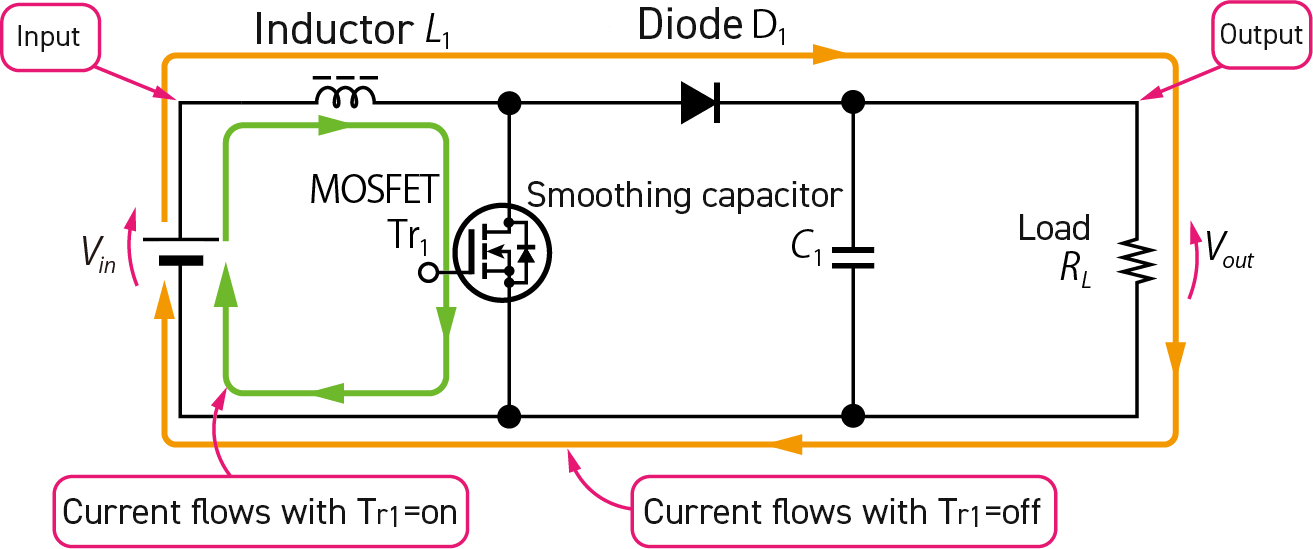
Figure 6: Basic circuit of boost DC-DC converter
Boost mechanism
The switch \( Tr_1 \), diode \( D_1 \), inductor \( L_1 \), and other components are the same as in the buck DC-DC converter, but the connections are different.
When \( Tr_1 \) turns on, \( L_1 \) is excited. When \( Tr_1 \) turns off, energy stored in \( L_1 \) is output through the diode. The current output by \( L_1 \) is smoothed by the capacitor \( C_1 \) to obtain a DC voltage.
Relationship between output voltage and PWM signal duty cycle
While \( Tr_1 \) is on, the input voltage is applied to \( L_1 \). The change \( \Delta I_L \) in the current in \( L_1 \) is expressed as follows.
\(\Delta I_L = \displaystyle \frac{V_{\text{in}}}{L_1} \times t_{\text{on}}\) (5)
Here \( \Delta I_L \) is the change (A) in the current in \( L_1 \) when \( Tr_1 \) is on, \( V_{IN} \) is the input voltage (V), \( L_1 \) is the inductance (H) of the inductor, and \( t_{on} \) is the on-time (s).
While \( Tr_1 \) is off, the difference \( V_{OUT} \) – \( V_{IN} \) between the output voltage and the input voltage is applied to \( L_1 \), as in the following equation.
\(\Delta I_L = \displaystyle \frac{V_{\text{out}} – V_{\text{in}}}{L_1} \times t_{\text{off}}\) (6)
Here \( t_{off} \) is the off-time (s).
While the output current is constant, the current change amounts \( \Delta I_L \) during the on-times and the off-times are equal.
From equations (5) and (6), we obtain the following equation (7) for the relationship between the output voltage of the boost DC-DC converter and the off duty cycle, which is the ratio of the off-time.
\(V_{\text{out}} = \displaystyle \frac{t_{\text{on}} + t_{\text{off}}}{t_{\text{off}}} \times V_{\text{in}}\) (7)
5. Isolated Flyback Converters Ideal for Small Power Supplies
Isolated DC-DC converters that supply energy to a load while providing DC isolation of the input (primary) side and the output (secondary) side are used in switching regulators that use commercial AC power supplies as input. Two types of circuit are used in isolated DC-DC converters; the timing of the currents flowing in the primary-side and secondary-side windings is different.
・Flyback converters
・Forward converters
The basic circuit of a flyback converter is shown below. Energy is stored in the transformer during intervals in which the primary side is conducting. When the primary side is shut off, energy is output from the secondary side. Flyback converters are widely used in isolated converters with relatively small capacity of 100 W or less.
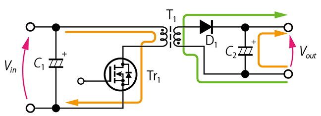
Figure 7. Isolated converter with small to intermediate capacity of up to 100 W
6. Forward Converters for Isolated DC-DC Converters Rated 100 W and Up
The basic circuit of a forward converter is shown below. A current flows in the primary (input) side of the transformer, and simultaneously a current flows in the secondary (output) side. This type of converter is used in large-capacity power supplies exceeding 100 W.
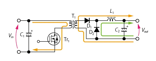
Figure 8: Isolated converter with large capacity of 100 W or more
7. Inverters that Convert DC to AC
An inverter is a circuit that converts direct current to alternating current and is used as a power control circuit to drive a motor. The basic circuit is shown below.
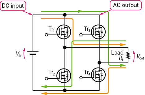
Figure 9: Basic configuration of inverter circuit
When a positive signal is output, \( Tr_1 \) and \( Tr_4 \) are turned on, while \( Tr_2 \) and \( Tr_3 \) are turned off. When outputting a negative signal, \( Tr_2 \) and \( Tr_3 \) are turned on, and \( Tr_1 \) and \( Tr_4 \) are turned off. The power transistors are driven to switch on and off at a high frequency that is tens to hundreds of times greater than the output frequency.
As shown in Figure 10, the on duty is made small near the zero-cross point at which the polarity of the output voltage changes, and is made large near where the output voltage is maximum. When this pulse signal is smoothed, a sine wave is obtained. Figure 11 shows an inverter circuit used to drive a 3-phase brushless motor.
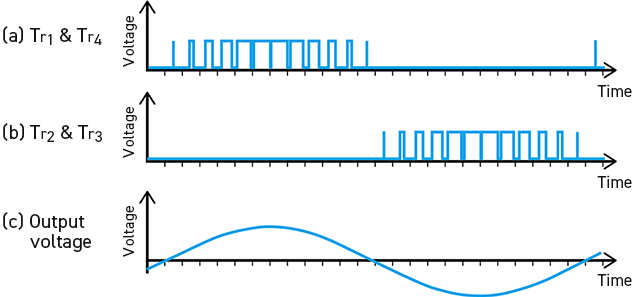
Figure 10: Operation of power transistors in inverter output stage and the sine wave
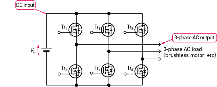
Figure 11: Inverter circuit to drive a 3-phase brushless motor
Supplemental: Power supply related terms that can be confusing
“Power supplies” are many and varied….
Power supplies are devices that extract electrical energy from batteries, generators, or other sources. Thermal (fuel-burning) power stations, AC power outlets, and dry-cell batteries are also “power supplies”. Different people will think of different things when the term “power supply” is used—such as power supply circuits, power supply units, power supply modules, or other systems or devices. The following is a summary of the devices that make up a power supply.
Power supply circuit
A power supply circuit is a series of circuits that converts an unstable voltage and current output by batteries into a stable voltage and current needed for electronic circuits and components such as motors to operate. A power supply circuit also includes linear regulators, switching regulators and other circuits.
- – A system that includes an AC-DC converter that converts AC power to DC.
- – A power supply unit that combines several types of circuits, including linear regulators and DC-DC converters.
Regulator
Regulators suppress input voltage fluctuations and generate a stable output voltage.
- -There are linear regulators and switching regulators, which use negative feedback to control the output voltage.
- -Regulator circuits are integrated into a single chip and offered as a linear regulator IC or switching regulator IC.
Linear regulator
Linear regulators provide a stable voltage by continuously operating current control elements such as transistors in an unsaturation region.
- – Designs combining transistors and resistors are possible.
- – Provided as a linear regulator IC that integrates control circuits and current control elements in one package.
Switching regulator
Switching regulators provide high-efficiency voltage conversion through high-speed ON/OFF operation of current control elements.
- – There are boost, buck, and buck-boost circuit types.
- – Provided as a switching regulator IC that integrates the circuits to control switching operation.
DC-DC converter
DC-DC converters convert a DC input voltage to a different DC voltage. The types of switching include buck, boost, and buck-boost. DC-DC converters feature high-efficiency conversion using switching operation.
- – Non-isolated: “DC-DC converter” itself often means a non-isolated device.
- – Isolated type: The primary and secondary sides are electrically separated by transformers, suitable for high-voltage environments and applications requiring safety. Typical examples are flyback converters and forward converters.
Inverter
Inverters are circuits that convert DC power to AC power and are widely used in motor driving and solar power generation systems.
- – An inverter employs a basic circuit technique that uses a switching operation to generate an AC signal.
- – Provided as a power supply unit for finished products used in motor driving and solar power generation systems.
【Download Documents】 Characteristics and Evaluation Method of Switching Regulators
This handbook reviews the basics of switching regulators and explains how to understand and evaluate the characteristics of switching regulators necessary for design optimization, along with reading and understanding the datasheets of switching regulator ICs.

DC-DC
Basic
- Operation During Shutdown of a Boost DC-DC Converter
- Linear Regulator Basics
-
Switching Regulator Basics
- Types of Switching Regulators
- Advantages vs Disadvantages in Comparison with Linear Regulator
- Supplement-Current Paths during Synchronous Rectifying Step-Down Converter Operation
- Operating Principles of Buck Switching Regulator
- Differences between Synchronous and Nonsynchronous Rectifying DC-DC Conversion
- Control Methods (Voltage Mode, Current Mode, Hysteresis Control)
- Efficiency Improvements at Light Load for the Synchronous Rectifying Type
- Protective and Sequencing Functions
- Considerations on Switching Frequencies
- Behavior when Vin Falls Below Vout
- Supplement-Protective Function: Output Pre-bias Protection
- Seven Representative Power Supply Circuits: From Low-noise to Boost Specs
- Concluding Remarks
- What is a DC/DC Converter?
Design
- Overview of Selection of Inductors and Capacitors for DC-DC Converters
-
Overview of DC-DC Converter PCB Layout
- Ringing at switching nodes
- Placement of input capacitors and output diodes
- Placement of Thermal Vias
- Placement of Inductors
- Placement of Output Capacitors
- Feedback Path Wiring
- Ground
- Resistance and Inductance of Copper Foil
- Noise countermeasures: corner wiring, conducted noise, radiated noise
- Noise countermeasures: snubber, bootstrap resistor, gate resistor
- Summary
-
PCB Layout of a Step-Up DC-DC Converter – Introduction
- The Importance of PCB Layout Design
- Current Paths in Step-up DC-DC Converters
- PCB Layout Procedure
- Placement of Input Capacitors
- Placement of Output Capacitors and Freewheel Diodes
- Inductor Placement
- Placement of Thermal Vias
- Feedback Path Wiring
- Ground
- Layout for Synchronous Rectification Designs
- Resistance and Inductance of Copper Foil
- Relationship Between Corner Wiring and Noise
- Summary
Evaluation
- Overview of Characteristics and Evaluation Method of Switching Regulators
- How to Read Power Supply IC Datasheets: Cover, Block Diagram, Absolute Maximum Ratings and Recommended Operating Conditions
- Evaluating a Switching Regulator: Output Voltage
-
Introduction
- Definitions and Heat Generation
- Losses in Synchronous Rectifying Step-Down Converters
- Conduction Losses in Synchronous Rectifying Step-Down Converters
- Switching Losses in Synchronous Rectifying Step-Down Converters
- Dead Time Losses in Synchronous Rectifying Step-Down Converters
- Controller IC Power Consumption Losses in a Synchronous Rectifying Step-Down Converter
- Gate Charge Losses in a Synchronous Rectifying Step-Down Converter
- Conduction Losses due to the Inductor DCR
- Example of Power Loss Calculation for a Power Supply IC
- Simplified Method of Loss Calculation
- Heat Calculation for Package Selection: Example 1
- Heat Calculation for Package Selection: Example 2
- Loss Factors
- Matters to Consider When Studying Miniaturization by Raising the Switching Frequency
- Important Matters when Studying High Input Voltage Applications
- Important Matters when Studying Large Output Currents Applications: Part 1
- Important Matters when Studying Large Output Currents Applications: Part 2
- Summary
Application
-
Important Points in the Design of a Power Supply Using a Linear Regulator
- Typical Application Circuit Examples of Linear Regulator ICs
- Input/output capacitor design and ripple prevention for linear regulator ICs
- How to determine efficiency and Thermal design for linear regulator ICs
- Protection of Linear Regulator IC Terminals
- Soft Starting of a Linear Regulator IC
- Overcurrent Protection(OCP) and Thermal Shutdown(TSD) of Linear Regulator IC
-
Important Points in the Design of a Power Supply Using a Floating Type Linear Regulator
- Example of Power Supply Circuit Based on a Floating Type Linear Regulator IC
- Input/output capacitor design and ripple prevention for linear regulator ICs
- How to determine efficiency and Thermal design for Floating Type Linear Regulator ICs
- Terminal protection for linear regulator ICs
- Startup characteristics for linear regulator ICs
- Failure to Start of a Power Supply Using a Linear Regulator, Case 1: Damage to the IC and Peripheral Components Due to Hand-Soldering
- About Parallel Connections of LDO Linear Regulators
-
Introduction
- Power Supply Sequence Specification ①: Power Supply Sequence Specifications and Control Block Diagrams
- Power Supply Sequence Specification①: Sequence Operation at Power Turn-on
- Power Supply Sequence Specification①: Sequence Operation at Power Shutoff
- Power Supply Sequence Specification①: Example of Actual Circuit and Component Value Calculations
- Power Supply Sequence Specification①: Example of Actual Operations
- Power Supply Sequence Specification②:Power Supply Sequence Specifications and Control Block Diagrams
- Power Supply Sequence Specification②:Sequence Operation at Power Turn-on
- Power Supply Sequence Specification②: Sequence Operation at Power Shutoff
- Power Supply Sequence Specification②: Example of Actual Circuit and Component Value Calculations
- Power Supply Sequence Specification②: Example of Actual Operations
- Circuits to Implement Power Supply Sequences Using General-Purpose Power Supply ICs ーSummaryー
- Easy Stabilization/Optimization Methods for Linear Regulators – Introduction
Product Information
FAQ