DC-DC|Application
About Step Response Method
2021.07.28
Points of this article
・Some linear regulators may oscillate when an MLCC or other low-ESR capacitor is used as the output capacitor.
・In such cases, a resistor can be inserted in series with the output capacitor to increase the apparent ESR and create a phase lead so as to avoid oscillation.
・One general approach to deciding the value of the resistor to insert in series is to determine the phase margin of the linear regulator in the circuit.
・As one measure to use when the phase margin cannot be measured, the step response method can be employed to easily confirm the stability of the linear regulator.
Linear regulators developed in an era in which multilayer ceramic capacitors (hereafter MLCCs) were not widely used may cause a phase lag in the feedback loop, leading to oscillation when a low-ESR capacitor such as an MLCC is connected to the output. In this case, a resistor can be inserted in series with the output capacitor to increase the apparent ESR and cause a phase lead, thereby avoiding oscillation.
One straightforward approach to determining the value of the resistor to be inserted in series is to determine the actual phase margin of the linear regulator in the circuit using a frequency response analyzer (FRA). However, it may not be possible to use an FRA, or even if an FRA is available for use, a linear regulator with a fixed output voltage may have its feedback loop within an IC where it cannot be accessed, so that the FRA cannot be used in phase margin measurements. One possible measure in such cases is using what is called the step response method to confirm and optimize the stability of the linear regulator by simple means.
About the Step Response Method
In the step response method, the output load (output current) is changed suddenly (stepped), and while using an oscilloscope to observe fluctuations in the output voltage (that is, the load transient response characteristic), adjustments are made to obtain a proper response. In this method, rigorous measurements of phase and gain are not possible, but even when using an FRA, the essence of the method is ultimately observation of the actual step response. In this sense, the method is empirically based, but can be considered to be an approach that depends on actual step responses.
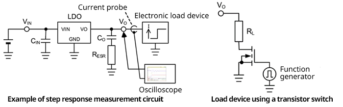
Below is shown an example of a circuit for step response measurement. The setup is comparatively simple. An electronic load device is connected to the output of the linear regulator, and the load current is changed suddenly, monitoring the load current and output voltage on an oscilloscope.
When an electronic load device is not available, measurements can also be performed using a circuit that employs a transistor switch. A function generator is connected to the gate of an N-channel MOSFET and the transistor is turned on and off at high speed. When the transistor is off the current is 0 A, and when it is on a current equal to VO÷RL flows.
The load current changes rapidly, for example from 0 A to the maximum output current of the linear regulator at a slew rate of 1 A/μs. Due to such sharp and large current steps, the output voltage essentially changes, stabilizing after a certain time has elapsed. The magnitude of this change and the time until convergence are optimized by adjusting the values of the relevant components (in this case, the value of RESR in the circuit diagram).
DC-DC
Basic
- Operation During Shutdown of a Boost DC-DC Converter
- Linear Regulator Basics
-
Switching Regulator Basics
- Types of Switching Regulators
- Advantages vs Disadvantages in Comparison with Linear Regulator
- Supplement-Current Paths during Synchronous Rectifying Step-Down Converter Operation
- Operating Principles of Buck Switching Regulator
- Differences between Synchronous and Nonsynchronous Rectifying DC-DC Conversion
- Control Methods (Voltage Mode, Current Mode, Hysteresis Control)
- Efficiency Improvements at Light Load for the Synchronous Rectifying Type
- Protective and Sequencing Functions
- Considerations on Switching Frequencies
- Behavior when Vin Falls Below Vout
- Supplement-Protective Function: Output Pre-bias Protection
- Seven Representative Power Supply Circuits: From Low-noise to Boost Specs
- Concluding Remarks
- What is a DC/DC Converter?
Design
- Overview of Selection of Inductors and Capacitors for DC-DC Converters
-
Overview of DC-DC Converter PCB Layout
- Ringing at switching nodes
- Placement of input capacitors and output diodes
- Placement of Thermal Vias
- Placement of Inductors
- Placement of Output Capacitors
- Feedback Path Wiring
- Ground
- Resistance and Inductance of Copper Foil
- Noise countermeasures: corner wiring, conducted noise, radiated noise
- Noise countermeasures: snubber, bootstrap resistor, gate resistor
- Summary
-
PCB Layout of a Step-Up DC-DC Converter – Introduction
- The Importance of PCB Layout Design
- Current Paths in Step-up DC-DC Converters
- PCB Layout Procedure
- Placement of Input Capacitors
- Placement of Output Capacitors and Freewheel Diodes
- Inductor Placement
- Placement of Thermal Vias
- Feedback Path Wiring
- Ground
- Layout for Synchronous Rectification Designs
- Resistance and Inductance of Copper Foil
- Relationship Between Corner Wiring and Noise
- Summary
Evaluation
- Overview of Characteristics and Evaluation Method of Switching Regulators
- How to Read Power Supply IC Datasheets: Cover, Block Diagram, Absolute Maximum Ratings and Recommended Operating Conditions
- Evaluating a Switching Regulator: Output Voltage
-
Introduction
- Definitions and Heat Generation
- Losses in Synchronous Rectifying Step-Down Converters
- Conduction Losses in Synchronous Rectifying Step-Down Converters
- Switching Losses in Synchronous Rectifying Step-Down Converters
- Dead Time Losses in Synchronous Rectifying Step-Down Converters
- Controller IC Power Consumption Losses in a Synchronous Rectifying Step-Down Converter
- Gate Charge Losses in a Synchronous Rectifying Step-Down Converter
- Conduction Losses due to the Inductor DCR
- Example of Power Loss Calculation for a Power Supply IC
- Simplified Method of Loss Calculation
- Heat Calculation for Package Selection: Example 1
- Heat Calculation for Package Selection: Example 2
- Loss Factors
- Matters to Consider When Studying Miniaturization by Raising the Switching Frequency
- Important Matters when Studying High Input Voltage Applications
- Important Matters when Studying Large Output Currents Applications: Part 1
- Important Matters when Studying Large Output Currents Applications: Part 2
- Summary
Application
-
Important Points in the Design of a Power Supply Using a Linear Regulator
- Typical Application Circuit Examples of Linear Regulator ICs
- Input/output capacitor design and ripple prevention for linear regulator ICs
- How to determine efficiency and Thermal design for linear regulator ICs
- Protection of Linear Regulator IC Terminals
- Soft Starting of a Linear Regulator IC
- Overcurrent Protection(OCP) and Thermal Shutdown(TSD) of Linear Regulator IC
-
Important Points in the Design of a Power Supply Using a Floating Type Linear Regulator
- Example of Power Supply Circuit Based on a Floating Type Linear Regulator IC
- Input/output capacitor design and ripple prevention for linear regulator ICs
- How to determine efficiency and Thermal design for Floating Type Linear Regulator ICs
- Terminal protection for linear regulator ICs
- Startup characteristics for linear regulator ICs
- Failure to Start of a Power Supply Using a Linear Regulator, Case 1: Damage to the IC and Peripheral Components Due to Hand-Soldering
- About Parallel Connections of LDO Linear Regulators
-
Introduction
- Power Supply Sequence Specification ①: Power Supply Sequence Specifications and Control Block Diagrams
- Power Supply Sequence Specification①: Sequence Operation at Power Turn-on
- Power Supply Sequence Specification①: Sequence Operation at Power Shutoff
- Power Supply Sequence Specification①: Example of Actual Circuit and Component Value Calculations
- Power Supply Sequence Specification①: Example of Actual Operations
- Power Supply Sequence Specification②:Power Supply Sequence Specifications and Control Block Diagrams
- Power Supply Sequence Specification②:Sequence Operation at Power Turn-on
- Power Supply Sequence Specification②: Sequence Operation at Power Shutoff
- Power Supply Sequence Specification②: Example of Actual Circuit and Component Value Calculations
- Power Supply Sequence Specification②: Example of Actual Operations
- Circuits to Implement Power Supply Sequences Using General-Purpose Power Supply ICs ーSummaryー
- Easy Stabilization/Optimization Methods for Linear Regulators – Introduction
Product Information
FAQ