DC-DC|Application
Power Supply Sequence Specification①: Example of Actual Circuit and Component Value Calculations
2022.02.24
Points of this article
・A circuit to realize the power supply sequence ① consists of 3 DCDCs, 4 Power Good blocks, 3 discharge circuits, and diodes.
In relation to the Power Supply Sequence Specification ①, in the article before the last and in the previous article, sequence operations upon power turn-on and shutoff were explained. In this article, an actual circuit example to realize these operations as well as component value calculations for circuit settings are explained.
Power Supply Sequence Specification①: Example of actual circuit and component value calculations
Below is shown an example of a circuit that realizes the power supply sequence. For the three DCDC systems 1 to 3, switching regulators or linear regulators (LDOs) are assumed. Each DCDC has an enable pin (EN) that can turn the output on and off.
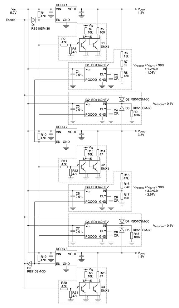
Example of a circuit to realize the Power Supply Sequence ①
●Power Good blocks
There are four Power Good blocks; a BD4142HFV, which is a voltage monitoring IC, is used to implement Power Good functions. IC1 and IC3 are used to detect the rise of the DCDC output voltage to the setting value at power turn-on, and IC2 and IC4 detect voltage drop at power shutoff. Below, a Power Good circuit that includes the BD4142HFV internal functional block is shown.
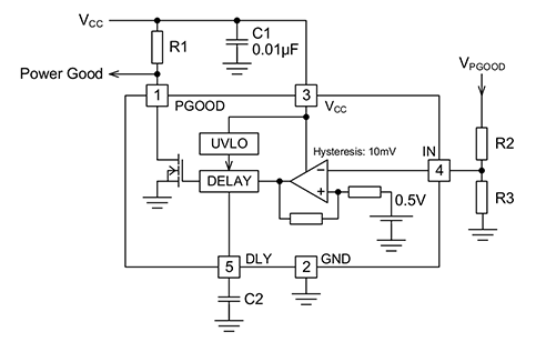
Power Good function using a BD4142HFV
This IC incorporates a hysteretic comparator with a 0.5 V reference voltage (see the IC functional block), and the voltage to be detected can be set using an external resistive divider. IC1 and IC3, which detect the rise of DCDC output voltages, must be set according to the DC-DC output voltages. The detection voltage VPGOOD can be calculated using equation 1-1.
![]()
In this sequence circuit example, VOUT1 is 1.2 V, and PGOOD of IC1 is set to output a flag when 90% of the output voltage is reached. If the detection voltage is set too high, such as at 95%, when the output voltage drops momentarily due to a load fluctuation the PGOOD output may go to “L”, so that a problem occurs when the later-stage DCDC is momentarily shut off. Detection voltages must be determined only after having understood DCDC load fluctuations and voltage drop (load response) characteristics.
At 90%, the detection voltage is 1.2 V × 0.9 = 1.08 V. The resistor value can be determined using equation 1-1. The calculated resistor values are already shown for IC1 in the circuit example; the resistance corresponding to R2 in equation 1-1 is R6 (15 kΩ) + R7 (82 Ω), and that corresponding to R3 is R8 (13 kΩ). Substituting these values, we see that they are the component values needed to obtain the desired 1.08 V.
![]()
As is seen from the equation, resistor values are determined relative to VPGOOD such that the voltage divided by R2 and R3 and applied to the IN pin is the internal reference voltage of 0.5 V. The voltage is determined by a resistor ratio, but this resistive voltage divider is also the DCDC load, and so it is appropriate to use resistor values in the 10 kΩ range. However, the sum of R2 and R3 is within 300 kΩ. For details, please refer to the data sheet.
Basic component values are determined in this way, but as part of design, tolerances for settings (detection voltages) must be confirmed. The detection voltage tolerance for the BD4142HFV is ±1.8%. Hence the range for PGOOD is from 88.4% (less than 90% by 1.8% of 90% = 90×0.982) to 91.6% (more than 90% by 1.8% of 90% = 90×1.018).
Moreover, there is a 10 mV hysteresis, so that the detection release voltage is 90%× (0.5 V – 10 mV)/0.5 V = 88.2%, and the range is 88.2%×0.982 = 86.6% to 88.2%×1.018 = 89.8%.
The BD4142HFV can impart a delay time tDELAY to the PGOOD flag output. In this case, a capacitor C2 is connected to the DLY pin. The delay time or the value of the capacitor C2 can be calculated using equation 1-2.
![]()
IC2 and IC4, the PGOOD pins of which operate upon power shutoff, release detection when the DCDC output voltage falls to about 0.5 V or lower (the PGOOD output changes from “H” to “L”). This utilizes the detection voltage, a basic setting in the BD4142HFV, without modification.
●Discharge circuit
Discretely configured discharge circuits are connected to the DCDCs. As indicated by the diagram below, the circuits consist of NPN transistors and resistors. The first-stage transistor is a simple inverter circuit; the second stage is an open-collector switch. Turn-on of the second stage causes the remaining charge, mainly in the output capacitor, to be discharged at DCDC shutoff, rapidly causing VOUT to fall. The fall time of the output voltage is adjusted through the value of the resistor (R4 in the diagram below) series-connected to the collector of the second-stage transistor.
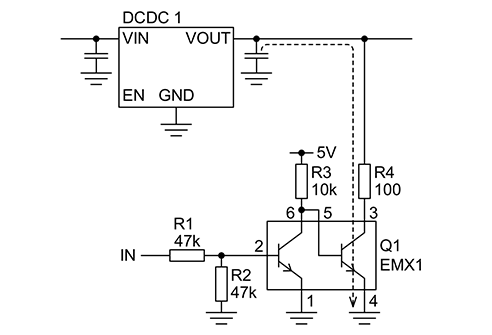
Discharge circuit
●Diodes
Diodes at different places in the sequence circuit are provided to govern logic operations. The forward voltage VF of a diode affects the voltage of an “L” level signal, and so a Schottky barrier diode with low VF is used to secure a “L” level voltage value.
The above has been an explanation of an entire circuit for realizing the Power Supply Sequence ①, as well as of Power Good blocks, discharge circuits and diodes which are peripheral circuits in addition to DCDCs.
DC-DC
Basic
- Operation During Shutdown of a Boost DC-DC Converter
- Linear Regulator Basics
-
Switching Regulator Basics
- Types of Switching Regulators
- Advantages vs Disadvantages in Comparison with Linear Regulator
- Supplement-Current Paths during Synchronous Rectifying Step-Down Converter Operation
- Operating Principles of Buck Switching Regulator
- Differences between Synchronous and Nonsynchronous Rectifying DC-DC Conversion
- Control Methods (Voltage Mode, Current Mode, Hysteresis Control)
- Efficiency Improvements at Light Load for the Synchronous Rectifying Type
- Protective and Sequencing Functions
- Considerations on Switching Frequencies
- Behavior when Vin Falls Below Vout
- Supplement-Protective Function: Output Pre-bias Protection
- Seven Representative Power Supply Circuits: From Low-noise to Boost Specs
- Concluding Remarks
- What is a DC/DC Converter?
Design
- Overview of Selection of Inductors and Capacitors for DC-DC Converters
-
Overview of DC-DC Converter PCB Layout
- Ringing at switching nodes
- Placement of input capacitors and output diodes
- Placement of Thermal Vias
- Placement of Inductors
- Placement of Output Capacitors
- Feedback Path Wiring
- Ground
- Resistance and Inductance of Copper Foil
- Noise countermeasures: corner wiring, conducted noise, radiated noise
- Noise countermeasures: snubber, bootstrap resistor, gate resistor
- Summary
-
PCB Layout of a Step-Up DC-DC Converter – Introduction
- The Importance of PCB Layout Design
- Current Paths in Step-up DC-DC Converters
- PCB Layout Procedure
- Placement of Input Capacitors
- Placement of Output Capacitors and Freewheel Diodes
- Inductor Placement
- Placement of Thermal Vias
- Feedback Path Wiring
- Ground
- Layout for Synchronous Rectification Designs
- Resistance and Inductance of Copper Foil
- Relationship Between Corner Wiring and Noise
- Summary
Evaluation
- Overview of Characteristics and Evaluation Method of Switching Regulators
- How to Read Power Supply IC Datasheets: Cover, Block Diagram, Absolute Maximum Ratings and Recommended Operating Conditions
- Evaluating a Switching Regulator: Output Voltage
-
Introduction
- Definitions and Heat Generation
- Losses in Synchronous Rectifying Step-Down Converters
- Conduction Losses in Synchronous Rectifying Step-Down Converters
- Switching Losses in Synchronous Rectifying Step-Down Converters
- Dead Time Losses in Synchronous Rectifying Step-Down Converters
- Controller IC Power Consumption Losses in a Synchronous Rectifying Step-Down Converter
- Gate Charge Losses in a Synchronous Rectifying Step-Down Converter
- Conduction Losses due to the Inductor DCR
- Example of Power Loss Calculation for a Power Supply IC
- Simplified Method of Loss Calculation
- Heat Calculation for Package Selection: Example 1
- Heat Calculation for Package Selection: Example 2
- Loss Factors
- Matters to Consider When Studying Miniaturization by Raising the Switching Frequency
- Important Matters when Studying High Input Voltage Applications
- Important Matters when Studying Large Output Currents Applications: Part 1
- Important Matters when Studying Large Output Currents Applications: Part 2
- Summary
Application
-
Important Points in the Design of a Power Supply Using a Linear Regulator
- Typical Application Circuit Examples of Linear Regulator ICs
- Input/output capacitor design and ripple prevention for linear regulator ICs
- How to determine efficiency and Thermal design for linear regulator ICs
- Protection of Linear Regulator IC Terminals
- Soft Starting of a Linear Regulator IC
- Overcurrent Protection(OCP) and Thermal Shutdown(TSD) of Linear Regulator IC
-
Important Points in the Design of a Power Supply Using a Floating Type Linear Regulator
- Example of Power Supply Circuit Based on a Floating Type Linear Regulator IC
- Input/output capacitor design and ripple prevention for linear regulator ICs
- How to determine efficiency and Thermal design for Floating Type Linear Regulator ICs
- Terminal protection for linear regulator ICs
- Startup characteristics for linear regulator ICs
- Failure to Start of a Power Supply Using a Linear Regulator, Case 1: Damage to the IC and Peripheral Components Due to Hand-Soldering
- About Parallel Connections of LDO Linear Regulators
-
Introduction
- Power Supply Sequence Specification ①: Power Supply Sequence Specifications and Control Block Diagrams
- Power Supply Sequence Specification①: Sequence Operation at Power Turn-on
- Power Supply Sequence Specification①: Sequence Operation at Power Shutoff
- Power Supply Sequence Specification①: Example of Actual Circuit and Component Value Calculations
- Power Supply Sequence Specification①: Example of Actual Operations
- Power Supply Sequence Specification②:Power Supply Sequence Specifications and Control Block Diagrams
- Power Supply Sequence Specification②:Sequence Operation at Power Turn-on
- Power Supply Sequence Specification②: Sequence Operation at Power Shutoff
- Power Supply Sequence Specification②: Example of Actual Circuit and Component Value Calculations
- Power Supply Sequence Specification②: Example of Actual Operations
- Circuits to Implement Power Supply Sequences Using General-Purpose Power Supply ICs ーSummaryー
- Easy Stabilization/Optimization Methods for Linear Regulators – Introduction
Product Information
FAQ