DC-DC|Design
Selection of Output Capacitors
2017.04.27
Points of this article
・When selecting an output capacitor, the rated voltage, rated ripple current, and ESR are important parameters.
・In addition to smoothing and regulation, output capacitors are also closely related to the output ripple voltage.
table of contents
In succession to selection of inductors, we turn to a discussion of capacitor selection. Capacitors that are essential for a step-down DC-DC converter include output capacitors and input capacitors. We begin by explaining output capacitors. Similarly to inductor selection, the choice of capacitor is also very important. Selection methods, recommended types and the like are essentially described in data sheets and related supporting materials, and these should be consulted.
Roles of input and output capacitors
First, in order to understand the roles of input capacitors and output capacitors, we review the current flows in a step-down DC-DC converter. By understanding the differences in the currents flowing in each capacitor, we will see what kinds of capacitors should be selected in each case.
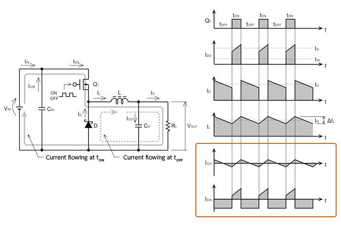
The same diagrams were used in “Basic Operation of Step-down Converters” in the waveforms enclosed in the rectangle, the upper waveform ICO and lower waveform ICIN are the current waveforms of the output and input capacitors respectively. The input capacitor is charged by VIN, and when the transistor Q1 turns on, discharges a current that becomes the switch current IDD. Comparatively high currents flow suddenly and repeatedly. The output capacitor is repeatedly charged and discharged according to the output ripple voltage, which is centered on the output voltage.
Selection of the output capacitor
From here, we discuss output capacitors. The following three factors are important when selecting the output capacitor.
1)Rated voltage
2)Rated ripple current
3)ESR (equivalent series resistance)
Of course the voltage and ripple current applied to a capacitor must be below the maximum ratings for the capacitor. The ESR is an important parameter that determines the output ripple voltage associated with the inductor current, and must be studied carefully.
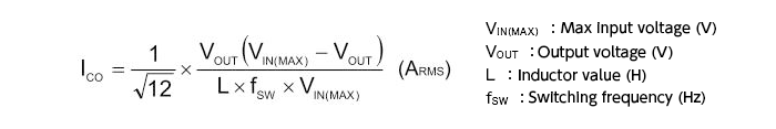
The ripple current of an output capacitor is a sawtooth wave, as indicated by ICO in the waveform diagram above; its effective value can be represented by the following equation.
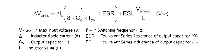
The output ripple voltage is represented by the following equation as the composite waveform resulting from the ripple component ΔIL of the inductor current IL in the above diagram, and the voltage occurring due to the capacitance, ESR, and ESL of the output capacitor.
When illustrated as waveforms, we obtain the following.
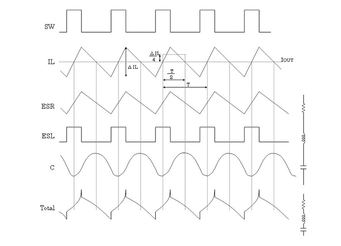
The ripple component ΔIL of the inductor current generated by switching causes a ripple voltage that is simply proportional to the ESR, and the ESL generates a square-wave voltage. The electrostatic capacitance component is combined with these to result in the final output ripple voltage waveform, shown at the bottom.
When representing the output ripple voltage, the following equation is used. Because the phases of the ripple due to the capacitor and the ripple due to the ESR are shifted, the two cannot simply be added together, but the following equation is often used to estimate the worst case value of the ripple voltage.

From this equation we see that in order to reduce the output ripple voltage, we should lower the ESR, increase the capacitance of the output capacitor, raise the switching frequency and reduce IL to the minimum necessary level.
In recent years, there appears to be a trend toward increased use of multilayer ceramic capacitors as output capacitors. Ceramic capacitors have extremely low ESR and ESL values, and so observed ripples originate almost entirely in the capacitance of the capacitor.
【Download Documents】 Switching Regulator Basics
The basics of step-down switching regulators, including their operation and functions, are explained. Comparison with linear regulators, synchronous rectification and diode rectification, control method, auxiliary functions, etc. are also explained.

DC-DC
Basic
- Operation During Shutdown of a Boost DC-DC Converter
- Linear Regulator Basics
-
Switching Regulator Basics
- Types of Switching Regulators
- Advantages vs Disadvantages in Comparison with Linear Regulator
- Supplement-Current Paths during Synchronous Rectifying Step-Down Converter Operation
- Operating Principles of Buck Switching Regulator
- Differences between Synchronous and Nonsynchronous Rectifying DC-DC Conversion
- Control Methods (Voltage Mode, Current Mode, Hysteresis Control)
- Efficiency Improvements at Light Load for the Synchronous Rectifying Type
- Protective and Sequencing Functions
- Considerations on Switching Frequencies
- Behavior when Vin Falls Below Vout
- Supplement-Protective Function: Output Pre-bias Protection
- Seven Representative Power Supply Circuits: From Low-noise to Boost Specs
- Concluding Remarks
- What is a DC/DC Converter?
Design
- Overview of Selection of Inductors and Capacitors for DC-DC Converters
-
Overview of DC-DC Converter PCB Layout
- Ringing at switching nodes
- Placement of input capacitors and output diodes
- Placement of Thermal Vias
- Placement of Inductors
- Placement of Output Capacitors
- Feedback Path Wiring
- Ground
- Resistance and Inductance of Copper Foil
- Noise countermeasures: corner wiring, conducted noise, radiated noise
- Noise countermeasures: snubber, bootstrap resistor, gate resistor
- Summary
-
PCB Layout of a Step-Up DC-DC Converter – Introduction
- The Importance of PCB Layout Design
- Current Paths in Step-up DC-DC Converters
- PCB Layout Procedure
- Placement of Input Capacitors
- Placement of Output Capacitors and Freewheel Diodes
- Inductor Placement
- Placement of Thermal Vias
- Feedback Path Wiring
- Ground
- Layout for Synchronous Rectification Designs
- Resistance and Inductance of Copper Foil
- Relationship Between Corner Wiring and Noise
- Summary
Evaluation
- Overview of Characteristics and Evaluation Method of Switching Regulators
- How to Read Power Supply IC Datasheets: Cover, Block Diagram, Absolute Maximum Ratings and Recommended Operating Conditions
- Evaluating a Switching Regulator: Output Voltage
-
Introduction
- Definitions and Heat Generation
- Losses in Synchronous Rectifying Step-Down Converters
- Conduction Losses in Synchronous Rectifying Step-Down Converters
- Switching Losses in Synchronous Rectifying Step-Down Converters
- Dead Time Losses in Synchronous Rectifying Step-Down Converters
- Controller IC Power Consumption Losses in a Synchronous Rectifying Step-Down Converter
- Gate Charge Losses in a Synchronous Rectifying Step-Down Converter
- Conduction Losses due to the Inductor DCR
- Example of Power Loss Calculation for a Power Supply IC
- Simplified Method of Loss Calculation
- Heat Calculation for Package Selection: Example 1
- Heat Calculation for Package Selection: Example 2
- Loss Factors
- Matters to Consider When Studying Miniaturization by Raising the Switching Frequency
- Important Matters when Studying High Input Voltage Applications
- Important Matters when Studying Large Output Currents Applications: Part 1
- Important Matters when Studying Large Output Currents Applications: Part 2
- Summary
Application
-
Important Points in the Design of a Power Supply Using a Linear Regulator
- Typical Application Circuit Examples of Linear Regulator ICs
- Input/output capacitor design and ripple prevention for linear regulator ICs
- How to determine efficiency and Thermal design for linear regulator ICs
- Protection of Linear Regulator IC Terminals
- Soft Starting of a Linear Regulator IC
- Overcurrent Protection(OCP) and Thermal Shutdown(TSD) of Linear Regulator IC
-
Important Points in the Design of a Power Supply Using a Floating Type Linear Regulator
- Example of Power Supply Circuit Based on a Floating Type Linear Regulator IC
- Input/output capacitor design and ripple prevention for linear regulator ICs
- How to determine efficiency and Thermal design for Floating Type Linear Regulator ICs
- Terminal protection for linear regulator ICs
- Startup characteristics for linear regulator ICs
- Failure to Start of a Power Supply Using a Linear Regulator, Case 1: Damage to the IC and Peripheral Components Due to Hand-Soldering
- About Parallel Connections of LDO Linear Regulators
-
Introduction
- Power Supply Sequence Specification ①: Power Supply Sequence Specifications and Control Block Diagrams
- Power Supply Sequence Specification①: Sequence Operation at Power Turn-on
- Power Supply Sequence Specification①: Sequence Operation at Power Shutoff
- Power Supply Sequence Specification①: Example of Actual Circuit and Component Value Calculations
- Power Supply Sequence Specification①: Example of Actual Operations
- Power Supply Sequence Specification②:Power Supply Sequence Specifications and Control Block Diagrams
- Power Supply Sequence Specification②:Sequence Operation at Power Turn-on
- Power Supply Sequence Specification②: Sequence Operation at Power Shutoff
- Power Supply Sequence Specification②: Example of Actual Circuit and Component Value Calculations
- Power Supply Sequence Specification②: Example of Actual Operations
- Circuits to Implement Power Supply Sequences Using General-Purpose Power Supply ICs ーSummaryー
- Easy Stabilization/Optimization Methods for Linear Regulators – Introduction
Product Information
FAQ