DC-DC|Design
Selection of Input Capacitors
2017.06.08
Points of this article
・Important issues in capacitor selection include the rated voltage, rated ripple current, characteristic for heat generation by ripples, and when using a ceramic capacitor, the temperature characteristic and DC bias characteristic in particular.
・Input capacitors must be able to tolerate higher voltages and currents than output capacitors.
table of contents
In the preceding section, we explained the role of output capacitors and important points in their selection. Next, we turn to an explanation of input capacitors. The following diagrams were also used in the section of output capacitors, but to aid understanding we use them again in an initial review of capacitor operation.
The Roles of Input and Output Capacitors
As in the previous section, we review the flow of currents in a DC-DC converter, and consider the nature of the currents flowing in the input and output capacitors.
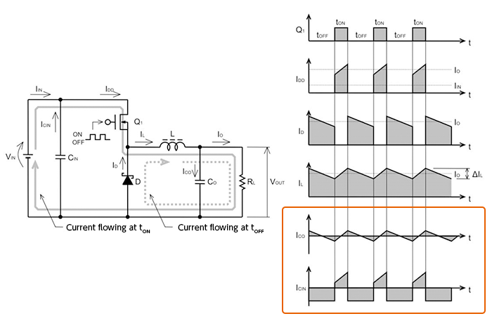
In the waveforms enclosed in the rectangle, the upper waveform ICO and the lower waveform ICIN are the current waveforms of the output and input capacitors respectively. The input capacitor is charged by VIN, and when the transistor Q1 turns on, discharges a current which becomes the switch current IDD. Comparatively high currents flow suddenly and repeatedly. In contrast, the output capacitor is repeatedly charged and discharged according to the output ripple voltage, which is centered on the output voltage; this difference should be kept in mind.
Selection of the input capacitor
The following three parameters are important when selecting the input capacitor.
1) Rated voltage
2) Rated ripple current and ripple heat generation characteristics
3) When using a ceramic capacitor: temperature characteristic and DC bias characteristic
Moreover, the following should be born in mind as premises for selection.
・The rated voltage must be higher than the maximum input voltage.
・The rated ripple current must be greater than the maximum input ripple current occurring in the IC input.
・In a step-down converter, the maximum value of the instantaneous input current is the same as the output current.
The effective value ICIN of the ripple current flowing in the input capacitor is represented by the following equation.

Based on this result, and using the absolute maximum rating of ripple current and a graph of the ripple heat generation characteristic, a capacitor with the required performance is selected.
The input ripple voltage ΔVIN can be calculated as follows.
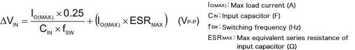
From this equation, we see that the input ripple voltage is smaller for larger values of the capacitance of the input capacitor.
A ceramic capacitor can be selected as an input capacitor. When using a ceramic capacitor, attention must generally be paid to temperature changes and to changes in capacitance due to the DC bias.
Where temperature characteristics are concerned, if the capacitor is a Class 2 (high dielectric constant) type, with an EAI code of X5R (-55 to +85°C, electrostatic capacitance changing rate ±15%) or X7R (-55 to +125°C, capacitance changing rate ±15%), then a sufficiently stable temperature characteristic can be obtained.
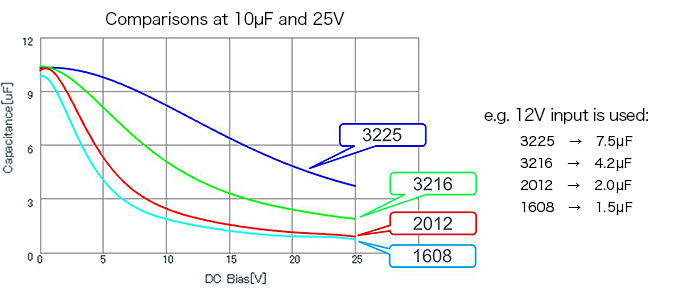
Where DC bias is concerned, of course a capacitor that is not greatly affected should be selected, but even for the same capacitance and voltage, fluctuation characteristics differ depending on the package size. The following graph illustrates some examples; capacitors with larger sizes exhibit less fluctuation. In any case, thorough information should be obtained from the capacitor manufacturer.
In essence, the input capacitor is selected on the basis of these parameters, but in trial manufacture and evaluation, checks must be performed to ensure that the input voltage with ripples added do not exceed the withstand voltage, and that heat generation caused by the ripple current can be tolerated.
【Download Documents】 Switching Regulator Basics
The basics of step-down switching regulators, including their operation and functions, are explained. Comparison with linear regulators, synchronous rectification and diode rectification, control method, auxiliary functions, etc. are also explained.

DC-DC
Basic
- Operation During Shutdown of a Boost DC-DC Converter
- Linear Regulator Basics
-
Switching Regulator Basics
- Types of Switching Regulators
- Advantages vs Disadvantages in Comparison with Linear Regulator
- Supplement-Current Paths during Synchronous Rectifying Step-Down Converter Operation
- Operating Principles of Buck Switching Regulator
- Differences between Synchronous and Nonsynchronous Rectifying DC-DC Conversion
- Control Methods (Voltage Mode, Current Mode, Hysteresis Control)
- Efficiency Improvements at Light Load for the Synchronous Rectifying Type
- Protective and Sequencing Functions
- Considerations on Switching Frequencies
- Behavior when Vin Falls Below Vout
- Supplement-Protective Function: Output Pre-bias Protection
- Seven Representative Power Supply Circuits: From Low-noise to Boost Specs
- Concluding Remarks
- What is a DC/DC Converter?
Design
- Overview of Selection of Inductors and Capacitors for DC-DC Converters
-
Overview of DC-DC Converter PCB Layout
- Ringing at switching nodes
- Placement of input capacitors and output diodes
- Placement of Thermal Vias
- Placement of Inductors
- Placement of Output Capacitors
- Feedback Path Wiring
- Ground
- Resistance and Inductance of Copper Foil
- Noise countermeasures: corner wiring, conducted noise, radiated noise
- Noise countermeasures: snubber, bootstrap resistor, gate resistor
- Summary
-
PCB Layout of a Step-Up DC-DC Converter – Introduction
- The Importance of PCB Layout Design
- Current Paths in Step-up DC-DC Converters
- PCB Layout Procedure
- Placement of Input Capacitors
- Placement of Output Capacitors and Freewheel Diodes
- Inductor Placement
- Placement of Thermal Vias
- Feedback Path Wiring
- Ground
- Layout for Synchronous Rectification Designs
- Resistance and Inductance of Copper Foil
- Relationship Between Corner Wiring and Noise
- Summary
Evaluation
- Overview of Characteristics and Evaluation Method of Switching Regulators
- How to Read Power Supply IC Datasheets: Cover, Block Diagram, Absolute Maximum Ratings and Recommended Operating Conditions
- Evaluating a Switching Regulator: Output Voltage
-
Introduction
- Definitions and Heat Generation
- Losses in Synchronous Rectifying Step-Down Converters
- Conduction Losses in Synchronous Rectifying Step-Down Converters
- Switching Losses in Synchronous Rectifying Step-Down Converters
- Dead Time Losses in Synchronous Rectifying Step-Down Converters
- Controller IC Power Consumption Losses in a Synchronous Rectifying Step-Down Converter
- Gate Charge Losses in a Synchronous Rectifying Step-Down Converter
- Conduction Losses due to the Inductor DCR
- Example of Power Loss Calculation for a Power Supply IC
- Simplified Method of Loss Calculation
- Heat Calculation for Package Selection: Example 1
- Heat Calculation for Package Selection: Example 2
- Loss Factors
- Matters to Consider When Studying Miniaturization by Raising the Switching Frequency
- Important Matters when Studying High Input Voltage Applications
- Important Matters when Studying Large Output Currents Applications: Part 1
- Important Matters when Studying Large Output Currents Applications: Part 2
- Summary
Application
-
Important Points in the Design of a Power Supply Using a Linear Regulator
- Typical Application Circuit Examples of Linear Regulator ICs
- Input/output capacitor design and ripple prevention for linear regulator ICs
- How to determine efficiency and Thermal design for linear regulator ICs
- Protection of Linear Regulator IC Terminals
- Soft Starting of a Linear Regulator IC
- Overcurrent Protection(OCP) and Thermal Shutdown(TSD) of Linear Regulator IC
-
Important Points in the Design of a Power Supply Using a Floating Type Linear Regulator
- Example of Power Supply Circuit Based on a Floating Type Linear Regulator IC
- Input/output capacitor design and ripple prevention for linear regulator ICs
- How to determine efficiency and Thermal design for Floating Type Linear Regulator ICs
- Terminal protection for linear regulator ICs
- Startup characteristics for linear regulator ICs
- Failure to Start of a Power Supply Using a Linear Regulator, Case 1: Damage to the IC and Peripheral Components Due to Hand-Soldering
- About Parallel Connections of LDO Linear Regulators
-
Introduction
- Power Supply Sequence Specification ①: Power Supply Sequence Specifications and Control Block Diagrams
- Power Supply Sequence Specification①: Sequence Operation at Power Turn-on
- Power Supply Sequence Specification①: Sequence Operation at Power Shutoff
- Power Supply Sequence Specification①: Example of Actual Circuit and Component Value Calculations
- Power Supply Sequence Specification①: Example of Actual Operations
- Power Supply Sequence Specification②:Power Supply Sequence Specifications and Control Block Diagrams
- Power Supply Sequence Specification②:Sequence Operation at Power Turn-on
- Power Supply Sequence Specification②: Sequence Operation at Power Shutoff
- Power Supply Sequence Specification②: Example of Actual Circuit and Component Value Calculations
- Power Supply Sequence Specification②: Example of Actual Operations
- Circuits to Implement Power Supply Sequences Using General-Purpose Power Supply ICs ーSummaryー
- Easy Stabilization/Optimization Methods for Linear Regulators – Introduction
Product Information
FAQ