DC-DC|Design
Resistance and Inductance of Copper Foil
2018.05.10
Points of this article
・Understand the basic construction of a printed circuit board.
・The resistance of copper foil layers appears as a voltage drop, and is dependent on temperature.
・The inductance of copper foil layers can in some cases generate high voltages, so care should be exercised.
・Shortening wiring lengths is effective for reducing inductance.
table of contents
PCB layout is important, but in addition to layout, it is also essential to understand the PC board and the copper foil layers themselves. This time, we will explain characteristics related to the board construction and materials, as well as the resistance and inductance of copper foil.
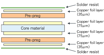
About PCB
The graphic on the right is a schematic diagram of the cross-section of a PCB. These are the basic construction and characteristics of a board, and so they should be remembered. The main points are listed below.
- Often the copper foil layers on the top and bottom surfaces are different in thickness from those on the inner layers.
- Often the copper foil layers on the core material are thicker, to increase heat dissipation.
- Core materials have general-use thicknesses, with the thickness adjusted using pre-preg.
- There are materials in which migration may occur, depending on the core material and the pre-preg type, and in some cases such materials cannot withstand high-humidity testing.
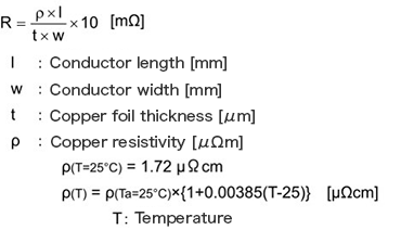
Resistance of Copper Foil
Of course, copper foil (wiring) has electrical resistance. Under conditions in which a large current flows, conduction losses, that is, a voltage drop and heat generation, occur. Hence where large-current lines are concerned, it is important to review the resistance values of copper foil layers.
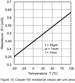
The resistance of copper foil is described as a value per unit area. Figure 10 indicates the resistance values per unit area of copper foil. The resistance values are for the generally application conditions of a copper foil thickness of 35 μm, width 1 mm, and length 1 mm.
The following equation is used for general calculations of resistance.
When calculating from the resistance value RP per unit area read off from Figure 10, we obtain the following.
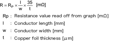
For example, at 25°C, the resistance value of copper foil of width 3 mm and length 50 mm, calculated as follows, is 8.17 mΩ.
![]()
From this resistance value, the voltage drop when a 3 A current flows is 24.5 mV. If the temperature rises to 100°C, from the graph we see that the resistance value increases 29%. Hence the voltage drop also increases, to 31.6 mV.
This voltage drop due to the copper foil can be a major problem, depending on circumstances. In essence, the wiring width should be studied in view of the current and temperature conditions.
Inductance of Copper Foil
As is also natural, copper foil has an inductance as well. It should be born in mind that parasitic components for resistance, capacitance, and inductance are always present.
The inductance of copper foil is expressed by the following equation.
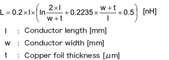
From this equation, we see that the inductance of copper foil depends hardly at all on the foil thickness.
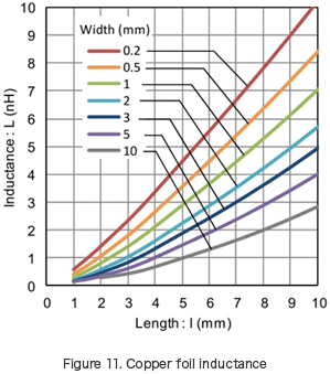
Figure 11 shows calculated values for copper foil inductance. As is clear from the graph, there is surprisingly little decrease in the inductance even when the line width is doubled.
In order to suppress the effects of parasitic inductance, the best approach is to shorten wiring lengths.
If the current propagating in printed wiring with inductance L (H) changes by i (A) in time t (s), then the following voltage appears across the ends of the printed wiring.
![]()
For example, if a 2 A current flows for 10 ns in printed wiring with a parasitic inductance of 6 nH, then the following voltage occurs.
![]()
Parasitic inductance can also cause large voltages, depending on the circumstances, and not only circuit operation can be affected, but components may be damaged or destroyed, so proper precautions must be taken.
【Download Documents】 DC-DC Buck Converter PCB Layout Basics
This hand book shows the basics and examples of board layout for DC-DC buck converters. It explains the concept and precautions of PCB layout, which also greatly affects the stability of switching type DC-DC converters.

DC-DC
Basic
- Operation During Shutdown of a Boost DC-DC Converter
- Linear Regulator Basics
-
Switching Regulator Basics
- Types of Switching Regulators
- Advantages vs Disadvantages in Comparison with Linear Regulator
- Supplement-Current Paths during Synchronous Rectifying Step-Down Converter Operation
- Operating Principles of Buck Switching Regulator
- Differences between Synchronous and Nonsynchronous Rectifying DC-DC Conversion
- Control Methods (Voltage Mode, Current Mode, Hysteresis Control)
- Efficiency Improvements at Light Load for the Synchronous Rectifying Type
- Protective and Sequencing Functions
- Considerations on Switching Frequencies
- Behavior when Vin Falls Below Vout
- Supplement-Protective Function: Output Pre-bias Protection
- Seven Representative Power Supply Circuits: From Low-noise to Boost Specs
- Concluding Remarks
- What is a DC/DC Converter?
Design
- Overview of Selection of Inductors and Capacitors for DC-DC Converters
-
Overview of DC-DC Converter PCB Layout
- Ringing at switching nodes
- Placement of input capacitors and output diodes
- Placement of Thermal Vias
- Placement of Inductors
- Placement of Output Capacitors
- Feedback Path Wiring
- Ground
- Resistance and Inductance of Copper Foil
- Noise countermeasures: corner wiring, conducted noise, radiated noise
- Noise countermeasures: snubber, bootstrap resistor, gate resistor
- Summary
-
PCB Layout of a Step-Up DC-DC Converter – Introduction
- The Importance of PCB Layout Design
- Current Paths in Step-up DC-DC Converters
- PCB Layout Procedure
- Placement of Input Capacitors
- Placement of Output Capacitors and Freewheel Diodes
- Inductor Placement
- Placement of Thermal Vias
- Feedback Path Wiring
- Ground
- Layout for Synchronous Rectification Designs
- Resistance and Inductance of Copper Foil
- Relationship Between Corner Wiring and Noise
- Summary
Evaluation
- Overview of Characteristics and Evaluation Method of Switching Regulators
- How to Read Power Supply IC Datasheets: Cover, Block Diagram, Absolute Maximum Ratings and Recommended Operating Conditions
- Evaluating a Switching Regulator: Output Voltage
-
Introduction
- Definitions and Heat Generation
- Losses in Synchronous Rectifying Step-Down Converters
- Conduction Losses in Synchronous Rectifying Step-Down Converters
- Switching Losses in Synchronous Rectifying Step-Down Converters
- Dead Time Losses in Synchronous Rectifying Step-Down Converters
- Controller IC Power Consumption Losses in a Synchronous Rectifying Step-Down Converter
- Gate Charge Losses in a Synchronous Rectifying Step-Down Converter
- Conduction Losses due to the Inductor DCR
- Example of Power Loss Calculation for a Power Supply IC
- Simplified Method of Loss Calculation
- Heat Calculation for Package Selection: Example 1
- Heat Calculation for Package Selection: Example 2
- Loss Factors
- Matters to Consider When Studying Miniaturization by Raising the Switching Frequency
- Important Matters when Studying High Input Voltage Applications
- Important Matters when Studying Large Output Currents Applications: Part 1
- Important Matters when Studying Large Output Currents Applications: Part 2
- Summary
Application
-
Important Points in the Design of a Power Supply Using a Linear Regulator
- Typical Application Circuit Examples of Linear Regulator ICs
- Input/output capacitor design and ripple prevention for linear regulator ICs
- How to determine efficiency and Thermal design for linear regulator ICs
- Protection of Linear Regulator IC Terminals
- Soft Starting of a Linear Regulator IC
- Overcurrent Protection(OCP) and Thermal Shutdown(TSD) of Linear Regulator IC
-
Important Points in the Design of a Power Supply Using a Floating Type Linear Regulator
- Example of Power Supply Circuit Based on a Floating Type Linear Regulator IC
- Input/output capacitor design and ripple prevention for linear regulator ICs
- How to determine efficiency and Thermal design for Floating Type Linear Regulator ICs
- Terminal protection for linear regulator ICs
- Startup characteristics for linear regulator ICs
- Failure to Start of a Power Supply Using a Linear Regulator, Case 1: Damage to the IC and Peripheral Components Due to Hand-Soldering
- About Parallel Connections of LDO Linear Regulators
-
Introduction
- Power Supply Sequence Specification ①: Power Supply Sequence Specifications and Control Block Diagrams
- Power Supply Sequence Specification①: Sequence Operation at Power Turn-on
- Power Supply Sequence Specification①: Sequence Operation at Power Shutoff
- Power Supply Sequence Specification①: Example of Actual Circuit and Component Value Calculations
- Power Supply Sequence Specification①: Example of Actual Operations
- Power Supply Sequence Specification②:Power Supply Sequence Specifications and Control Block Diagrams
- Power Supply Sequence Specification②:Sequence Operation at Power Turn-on
- Power Supply Sequence Specification②: Sequence Operation at Power Shutoff
- Power Supply Sequence Specification②: Example of Actual Circuit and Component Value Calculations
- Power Supply Sequence Specification②: Example of Actual Operations
- Circuits to Implement Power Supply Sequences Using General-Purpose Power Supply ICs ーSummaryー
- Easy Stabilization/Optimization Methods for Linear Regulators – Introduction
Product Information
FAQ