DC-DC|Design
Resistance and Inductance of Copper Foil
2021.06.09
Points of this article
・The resistance of copper foil appears as a drop in voltage, and depends on the temperature.
・The inductance of copper foil can result in high voltages under some circumstances, thus requiring caution.
・Shortening wiring lengths is effective to reduce inductances.
table of contents
This article explains the resistance and inductance of copper foil. The comments here are not limited to the case of step-up DC-DC converters, but apply to PCBs in general, and so should be considered part of basic knowledge of PCB layout.
Resistance of Copper Foil
The copper foil that is metal trace on a PCB has electrical resistance. When a large current flows, conduction losses result in a voltage drop and heat generation. A wiring line in which large currents flow must be studied to determine the resistance value of the copper foil.
Normally, the resistance of copper foil is considered in area units. The following graph shows the resistance value per unit area of copper foil. Here the resistance values are for general copper foil of thickness 35 μm, width 1 mm, and length 1 mm. The resistance value can be calculated using the formula below.

Using the resistance value per unit area RP read off from the graph, the formula can be modified as follows. For example, we see that at 25°C, the resistance value of copper foil of width 3 mm and length 50 mm is 8.17 mΩ, as indicated by the equation on the lower right.
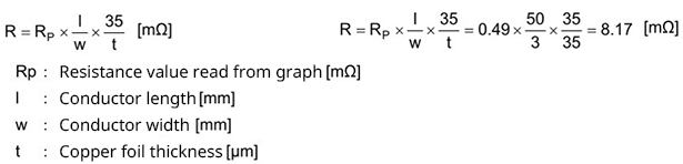
In this example, the voltage drop when a 3 A current is flowing is 24.5 mV. From the graph, when the temperature rises to 100°C, RP increases to 0.63 mΩ, and the voltage drop increases to 31.6 mV. This is an increase of about 29%. When such a voltage drop due to copper foil cannot be allowed, in essence, the wiring width is examined.
Inductance of Copper Foil
Copper foil has an inductance. The inductance of copper foil can be represented by the following formula. A graph is also shown that plots the inductance obtained using this formula when, for wiring widths of 0.2 mm to 10 mm, the wiring length is changed.
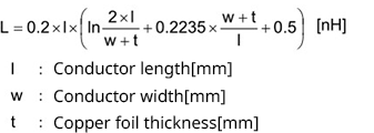
From the equation, we see that the inductance hardly depends at all on the copper foil thickness. Moreover, from the graph it is clear that even when the wiring width is doubled, there is surprisingly little decrease in the inductance. Consequently, we see that in order to suppress the inductance of copper foil, shortening the wiring length is effective.
If the current flowing in printed wiring with inductance L (H) changes by i (A) over time t (s), then the following voltage appears across the ends of the printed wiring.
![]()
For example, when a 2 A current flows for 10 ns in printed wiring with an inductance of 6 nH, the voltage generated is as follows.
![]()
The parasitic inductance of wiring not only generates large voltages under some conditions to affect operation, but in some cases can cause component failure, and so appropriate caution is necessary.
【Download Documents】 Linear Regulator Basics
This is a hand book for understanding the basics of linear regulators, such as operating principles, classification, characteristics by circuit configuration, advantages and disadvantages. In addition, typical specifications of linear regulators, efficiency and thermal calculations are also explained.

DC-DC
Basic
- Operation During Shutdown of a Boost DC-DC Converter
- Linear Regulator Basics
-
Switching Regulator Basics
- Types of Switching Regulators
- Advantages vs Disadvantages in Comparison with Linear Regulator
- Supplement-Current Paths during Synchronous Rectifying Step-Down Converter Operation
- Operating Principles of Buck Switching Regulator
- Differences between Synchronous and Nonsynchronous Rectifying DC-DC Conversion
- Control Methods (Voltage Mode, Current Mode, Hysteresis Control)
- Efficiency Improvements at Light Load for the Synchronous Rectifying Type
- Protective and Sequencing Functions
- Considerations on Switching Frequencies
- Behavior when Vin Falls Below Vout
- Supplement-Protective Function: Output Pre-bias Protection
- Seven Representative Power Supply Circuits: From Low-noise to Boost Specs
- Concluding Remarks
- What is a DC/DC Converter?
Design
- Overview of Selection of Inductors and Capacitors for DC-DC Converters
-
Overview of DC-DC Converter PCB Layout
- Ringing at switching nodes
- Placement of input capacitors and output diodes
- Placement of Thermal Vias
- Placement of Inductors
- Placement of Output Capacitors
- Feedback Path Wiring
- Ground
- Resistance and Inductance of Copper Foil
- Noise countermeasures: corner wiring, conducted noise, radiated noise
- Noise countermeasures: snubber, bootstrap resistor, gate resistor
- Summary
-
PCB Layout of a Step-Up DC-DC Converter – Introduction
- The Importance of PCB Layout Design
- Current Paths in Step-up DC-DC Converters
- PCB Layout Procedure
- Placement of Input Capacitors
- Placement of Output Capacitors and Freewheel Diodes
- Inductor Placement
- Placement of Thermal Vias
- Feedback Path Wiring
- Ground
- Layout for Synchronous Rectification Designs
- Resistance and Inductance of Copper Foil
- Relationship Between Corner Wiring and Noise
- Summary
Evaluation
- Overview of Characteristics and Evaluation Method of Switching Regulators
- How to Read Power Supply IC Datasheets: Cover, Block Diagram, Absolute Maximum Ratings and Recommended Operating Conditions
- Evaluating a Switching Regulator: Output Voltage
-
Introduction
- Definitions and Heat Generation
- Losses in Synchronous Rectifying Step-Down Converters
- Conduction Losses in Synchronous Rectifying Step-Down Converters
- Switching Losses in Synchronous Rectifying Step-Down Converters
- Dead Time Losses in Synchronous Rectifying Step-Down Converters
- Controller IC Power Consumption Losses in a Synchronous Rectifying Step-Down Converter
- Gate Charge Losses in a Synchronous Rectifying Step-Down Converter
- Conduction Losses due to the Inductor DCR
- Example of Power Loss Calculation for a Power Supply IC
- Simplified Method of Loss Calculation
- Heat Calculation for Package Selection: Example 1
- Heat Calculation for Package Selection: Example 2
- Loss Factors
- Matters to Consider When Studying Miniaturization by Raising the Switching Frequency
- Important Matters when Studying High Input Voltage Applications
- Important Matters when Studying Large Output Currents Applications: Part 1
- Important Matters when Studying Large Output Currents Applications: Part 2
- Summary
Application
-
Important Points in the Design of a Power Supply Using a Linear Regulator
- Typical Application Circuit Examples of Linear Regulator ICs
- Input/output capacitor design and ripple prevention for linear regulator ICs
- How to determine efficiency and Thermal design for linear regulator ICs
- Protection of Linear Regulator IC Terminals
- Soft Starting of a Linear Regulator IC
- Overcurrent Protection(OCP) and Thermal Shutdown(TSD) of Linear Regulator IC
-
Important Points in the Design of a Power Supply Using a Floating Type Linear Regulator
- Example of Power Supply Circuit Based on a Floating Type Linear Regulator IC
- Input/output capacitor design and ripple prevention for linear regulator ICs
- How to determine efficiency and Thermal design for Floating Type Linear Regulator ICs
- Terminal protection for linear regulator ICs
- Startup characteristics for linear regulator ICs
- Failure to Start of a Power Supply Using a Linear Regulator, Case 1: Damage to the IC and Peripheral Components Due to Hand-Soldering
- About Parallel Connections of LDO Linear Regulators
-
Introduction
- Power Supply Sequence Specification ①: Power Supply Sequence Specifications and Control Block Diagrams
- Power Supply Sequence Specification①: Sequence Operation at Power Turn-on
- Power Supply Sequence Specification①: Sequence Operation at Power Shutoff
- Power Supply Sequence Specification①: Example of Actual Circuit and Component Value Calculations
- Power Supply Sequence Specification①: Example of Actual Operations
- Power Supply Sequence Specification②:Power Supply Sequence Specifications and Control Block Diagrams
- Power Supply Sequence Specification②:Sequence Operation at Power Turn-on
- Power Supply Sequence Specification②: Sequence Operation at Power Shutoff
- Power Supply Sequence Specification②: Example of Actual Circuit and Component Value Calculations
- Power Supply Sequence Specification②: Example of Actual Operations
- Circuits to Implement Power Supply Sequences Using General-Purpose Power Supply ICs ーSummaryー
- Easy Stabilization/Optimization Methods for Linear Regulators – Introduction
Product Information
FAQ